In this tutorial, we will learn to use SPI communication modules of TM4C123 microcontroller using Tiva C Launchpad. As per the nomenclature of the TM4C123GH6PM microcontroller, the name used for SPI modules is a synchronous serial interface(SSI). But it is popularly referred to as a serial peripheral interface. That is why we will use the term SPI instead of SSI throughout this tutorial. Because SSI modules support three protocols such as TI serial interface, MICROWIRE, and SPI. First, we will learn to configure SPI modules through their registers. In the end, we will see an example of SPI communication between TM4C123G Tiva Launchpad and Arduino.
Pre-requisites:
- How to Download and Install Keil uVision for ARM and 8051
- Getting started with Keil uVision: Write your first Program for Tiva LaunchPad
TM4C123 SPI Modules
As you know that Tiva Launchpad comes with TM4C123GF6PM microcontroller. This microcontroller contains four serial peripheral interfaces or SPI modules. Each module can be configured in master or slave mode to receive or send data to other devices that communicate over SPI interface.SSI modules convert serial data into parallel data.

Followings are the main features of TM4C123 SPI modules:
- Master and Slave Configuration
- FIFOs for each SPI transmitter and receiver
- Direct SPI data transfer to DMA ( direct memory access controller)
In this modern embedded systems era, many sensors such as mcp3008, ADCs, DACs, Temperature and pressure sensors etc, provide data over SPI communication. This way we can take off processor and microcontroller load of data acquisition and directly take data measurements from these sensors through SPI communication.
SPI Modules Pins
As we mentioned earlier, TM4C123 microcontroller has four SPI modules. In order for SPI based devices to communicate with each other, four pins are required such as clock, serial data in, serial data out and frame signal. This table lists the external signals of each SPI module on GPIO pins of TM4C123 Tiva Launchpad.
| Pin Name | GPIO Pin | SPI Module |
|---|---|---|
| SSI0CLK | PA2 | SPI0 |
| SSI0Fss | PA3 | SPI0 |
| SSI0Rx | PA4 | SPI0 |
| SSI0Tx | PA5 | SPI0 |
| SSI1CLK | PF2/PD0 | SPI1 |
| SSI1Fss | PF3/PD1 | SPI1 |
| SSI1Rx | PF0/PD2 | SPI1 |
| SSI1Tx | PF1/PD3 | SPI1 |
| SSI2CLK | PB4 | SPI2 |
| SSI2Fss | PB5 | SPI2 |
| SSI2Rx | PB6 | SPI2 |
| SSI2Tx | PB7 | SPI2 |
| SSI3CLK | PD0 | SPI3 |
| SSI3Fss | PD1 | SPI3 |
| SSI2Rx | PD2 | SPI3 |
| SSI3Tx | PD3 | SPI3 |
TM4C123 SPI Configuration Registers
These registers are used to configure SPI modules of TM4C123 in master and slave mode. This table lists configuration registers and their functions.
| Register Name | Function |
|---|---|
| RCGCSSI | Enable SPI module |
| RCGCGPIO | Enable Clock to respective pins used for SPI communication |
| GPIOAFSEL | Enable alternative function of GPIO pins |
| GPIOPCTL | Select alternate function of GPIO pins for SPI communication |
| GPIODEN | Set GPIO pins as digital pins |
| SSICR1 | Used to enable SPI module and master/slave configuration |
| SSICC | Enable system clock frequency to SPI module |
| SSICPSR | System clock pre-divisor setting |
| SSICR0 | Define clock rate, phase and polarity, protocol mode |
TM4C123 SPI Communication Code
This example code demonstrates the use of the SSI1 module of TM4C123GH6PM microcontroller in SPI mode. According to the above table, GPIO pins RD0, RD2, RD3 can be configured as CLK, transmit and receive pin for SPI1 communication module.
This code initializes and configures SPI1 module in master mode operating
at 4MHz clock frequency. In addition, 8-bit data size, mode 0 of SPI frame format are also configured.
Inside the while loop, TM4C123 microntroller transmits character ‘A’ through SSI1Tx pin and waits for one second. After that, it transmits character ‘B’ and waits again for one second.
/* Example code to transmit data with SPI1 module of TM4C123 */
/* Transmits character A and B with a delay of one second */
#include "TM4C123GH6PM.h"

/* function prototype of SPI and Delay */
void SPI1_init(void);
void SPI1_Write(unsigned char data);
void Delay_ms(int time_ms);

/* Main routine of code */
int main(void)
{
    unsigned char val1 = 'A';
	  unsigned char val2 = 'B';

    SPI1_init();
    while(1)
		{
    SPI1_Write(val1); /* write a character */
    Delay_ms(1000);
		SPI1_Write(val2); /* write a character */
    Delay_ms(1000);
    }
}

void SPI1_Write(unsigned char data)
{
    GPIOF->DATA &= ~(1<<2);       /* Make PF2 Selection line (SS) low */
    while((SSI1->SR & 2) == 0); /* wait untill Tx FIFO is not full */
    SSI1->DR = data;            /* transmit byte over SSI1Tx line */
    while(SSI1->SR & 0x10);     /* wait until transmit complete */
    GPIOF->DATA |= 0x04;        /* keep selection line (PF2) high in idle condition */
}

void SPI1_init(void)
{
    /* Enable clock to SPI1, GPIOD and GPIOF */

   	SYSCTL->RCGCSSI |= (1<<1);   /*set clock enabling bit for SPI1 */
    SYSCTL->RCGCGPIO |= (1<<3); /* enable clock to GPIOD for SPI1 */
    SYSCTL->RCGCGPIO |= (1<<5); /* enable clock to GPIOF for slave select */

    /*Initialize PD3 and PD0 for SPI1 alternate function*/

    GPIOD->AMSEL &= ~0x09;      /* disable analog functionality RD0 and RD3 */
    GPIOD->DEN |= 0x09;         /* Set RD0 and RD3 as digital pin */
    GPIOD->AFSEL |= 0x09;       /* enable alternate function of RD0 and RD3*/
    GPIOD->PCTL &= ~0x0000F00F; /* assign RD0 and RD3 pins to SPI1 */
    GPIOD->PCTL |= 0x00002002;  /* assign RD0 and RD3 pins to SPI1  */

    /* Initialize PF2 as a digital output as a slave select pin */

    GPIOF->DEN |= (1<<2);         /* set PF2 pin digital */
    GPIOF->DIR |= (1<<2);         /* set PF2 pin output */
    GPIOF->DATA |= (1<<2);        /* keep SS idle high */

    /* Select SPI1 as a Master, POL = 0, PHA = 0, clock = 4 MHz, 8 bit data */

    SSI1->CR1 = 0;          /* disable SPI1 and configure it as a Master */
    SSI1->CC = 0;           /* Enable System clock Option */
    SSI1->CPSR = 4;         /* Select prescaler value of 4 .i.e 16MHz/4 = 4MHz */
    SSI1->CR0 = 0x00007;     /* 4MHz SPI1 clock, SPI mode, 8 bit data */
    SSI1->CR1 |= 2;         /* enable SPI1 */
}

/* This function generates delay in ms */
/* calculations are based on 16MHz system clock frequency */

void Delay_ms(int time_ms)
{
    int i, j;
    for(i = 0 ; i < time_ms; i++)
        for(j = 0; j < 3180; j++)
            {}  /* excute NOP for 1ms */
}

void SystemInit(void)
{
    /* use this only if you are using old versions of Keil uvision */
    SCB->CPACR |= 0x00f00000;
}
For SPI master and slave devices to communicate with each other, they should have common parameters such as clock frequency, phase, SPHA, SPOL. In this TM4C123 SPI code, we configure SPI1 as a Master and operating frequency of 4MHz with POL = 0, PHA = 0.
The reason we have chosen 4MHz frequency and both phase zero. Because we want to communicate between TM4C123 Tiva Launchpad and Arduino. The default parameters settings for Arduino SPI module are POL = 0, PHA = 0, clock = 4 MHz. Therefore, it makes parameters for both master and slave devices common.
How Does Code Work?
The code demonstrates SPI data transmission using the SPI1 module of the TM4C123 microcontroller. The characters ‘A’ and ‘B’ are sent alternately with a delay of one second between transmissions. Here’s how the code works:
Here’s a more detailed explanation of how the code works:
1. Main Routine (main)
The main() function serves as the core loop where SPI transmission occurs. The characters ‘A’ and ‘B’ are alternately transmitted via SPI with a 1-second delay between them. This process runs continuously in an infinite loop.
int main(void)
{
    unsigned char val1 = 'A';  // Character to send first
    unsigned char val2 = 'B';  // Character to send next

    SPI1_init();  // Initialize the SPI1 module and related GPIO pins
    while(1)
    {
        SPI1_Write(val1); // Transmit character 'A' through SPI
        Delay_ms(1000);   // Wait for 1 second
        SPI1_Write(val2); // Transmit character 'B' through SPI
        Delay_ms(1000);   // Wait for 1 second
    }
}
2. SPI Data Transmission (SPI1_Write)
The SPI1_Write() function handles transmitting data via the SPI1 module. It controls the slave select (SS) line connected to GPIO pin PF2, signaling the start and end of data transmission. This line is set low before sending the data (to enable communication with the slave device) and set high after the transmission completes (to indicate the end of communication).
- GPIOF->DATA &= ~(1<<2): Pulls PF2 low to enable communication with the slave (activating SS).
- while((SSI1->SR & 2) == 0): Waits until the transmit FIFO (buffer) is not full before sending data.
- SSI1->DR = data: Loads the data into the data register, triggering transmission over the MOSI (Master Out Slave In) line.
- while(SSI1->SR & 0x10): Waits for the transmission to complete.
- GPIOF->DATA |= 0x04: Sets PF2 high again, signaling the end of communication.
void SPI1_Write(unsigned char data)
{
    GPIOF->DATA &= ~(1<<2);       // Set SS low to begin communication
    while((SSI1->SR & 2) == 0);   // Wait until the transmit FIFO is ready
    SSI1->DR = data;              // Transmit the data byte via SPI
    while(SSI1->SR & 0x10);       // Wait until transmission is complete
    GPIOF->DATA |= 0x04;          // Set SS high to end communication
}
3. SPI1 Initialization (SPI1_init)
This function sets up the SPI1 module and configures the necessary GPIO pins. It enables clocks for the SPI1 module, configures pins PD0 and PD3 for SPI functionality, and sets up PF2 as the slave select (SS) pin.
- SYSCTL->RCGCSSI |= (1<<1): Enables the clock for the SPI1 module.
- SYSCTL->RCGCGPIO |= (1<<3): Enables the clock for GPIO port D (for SPI pins).
- SYSCTL->RCGCGPIO |= (1<<5): Enables the clock for GPIO port F (for SS pin).
- GPIOD->DEN, AFSEL, PCTL: Configures PD0 and PD3 as digital pins for SPI1 alternate functionality (PD0 = SPI1Clk, PD3 = SPI1Tx).
- GPIOF->DEN, DIR, DATA: Configures PF2 as an output pin for controlling the slave select (SS) line. It is set high by default (SS inactive).
- SSI1->CR1, CC, CPSR, CR0: Configures the SPI1 module in master mode, sets the clock speed to 4 MHz, selects SPI mode (POL = 0, PHA = 0), and specifies 8-bit data transfer.
void SPI1_init(void)
{
    // Enable clock for SPI1, GPIOD, and GPIOF
    SYSCTL->RCGCSSI |= (1<<1);    // Enable clock for SPI1
    SYSCTL->RCGCGPIO |= (1<<3);   // Enable clock for GPIOD (SPI pins)
    SYSCTL->RCGCGPIO |= (1<<5);   // Enable clock for GPIOF (SS pin)

    // Configure PD0 and PD3 for SPI1
    GPIOD->AMSEL &= ~0x09;        // Disable analog function on PD0 and PD3
    GPIOD->DEN |= 0x09;           // Enable digital function on PD0 and PD3
    GPIOD->AFSEL |= 0x09;         // Enable alternate function for PD0 and PD3
    GPIOD->PCTL &= ~0x0000F00F;   // Clear PCTL for PD0 and PD3
    GPIOD->PCTL |= 0x00002002;    // Assign PD0 and PD3 to SPI1

    // Configure PF2 as a digital output for SS (Slave Select)
    GPIOF->DEN |= (1<<2);         // Enable digital function on PF2
    GPIOF->DIR |= (1<<2);         // Set PF2 as output
    GPIOF->DATA |= (1<<2);        // Set PF2 high (SS inactive)

    // Set SPI1 as master, mode 0 (POL=0, PHA=0), 8-bit data, 4 MHz clock
    SSI1->CR1 = 0;                // Disable SPI1 and set master mode
    SSI1->CC = 0;                 // Use system clock
    SSI1->CPSR = 4;               // Set clock prescaler to 4 (16 MHz / 4 = 4 MHz)
    SSI1->CR0 = 0x00007;          // Set clock, SPI mode, 8-bit data
    SSI1->CR1 |= 2;               // Enable SPI1
}
4. Delay Function (Delay_ms)
The Delay_ms() function creates a software delay. It is based on a simple loop that runs for the calculated number of iterations to produce a delay. The inner loop (for(j = 0; j < 3180; j++)) runs 3180 times, which approximately equates to 1 millisecond for the TM4C123 running at 16 MHz.
void Delay_ms(int time_ms)
{
    int i, j;
    for(i = 0; i < time_ms; i++)  // Outer loop for the number of milliseconds
        for(j = 0; j < 3180; j++) // Inner loop to generate delay for 1 ms
            {}  // Empty loop (NOP) for creating delay
}
5. System Initialization (SystemInit)
The SystemInit() function is provided for compatibility with older versions of the Keil IDE. It configures the floating-point unit by setting bits in the CPACR register. This step is only needed in specific cases when working with older versions of the development environment.
void SystemInit(void)
{
    SCB->CPACR |= 0x00f00000;  // Enable the floating-point unit (if needed)
}
Summary
- Initialization: The
SPI1_init()function configures the SPI1 module in master mode, sets up the SPI clock at 4 MHz, and assigns the appropriate GPIO pins for SPI communication. - Data Transmission: The
SPI1_Write()function transmits characters ‘A’ and ‘B’ alternately via SPI, controlling the slave select (SS) pin to manage communication with the SPI slave device. - Delays: The
Delay_ms()function introduces a delay of 1 second between each transmission, creating a noticeable gap between successive characters.
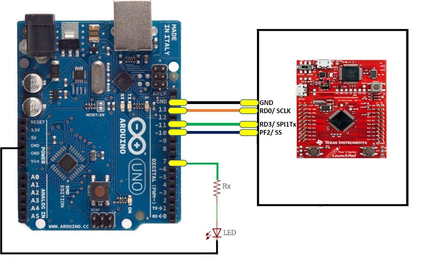
SPI Communication with Arduino and TM4C123 Tiva Launchpad
To see the demonstration of the above code, we will perform SPI communication with TM4C123 Tiva Launchpad and Arduino. Tiva Launchpad will be configured as a master device and Arduino as a slave device.
Arduino as a SPI Slave Device
In this example code of Arduino, Arduino acts as a slave device.
#include<SPI.h>
#define LEDpin 7
volatile boolean received;
char Slavereceived;
void setup()
{
  Serial.begin(9600);
  pinMode(LEDpin,OUTPUT);                 // Setting pin 7 as OUTPU
  SPCR |= (1<<SPE)| (1<<SPIE);            //Turn on SPI in Slave Mode
  received = false;
  SPI.attachInterrupt();                  //Interuupt ON is set for SPI commnucation
  sei();
}

ISR (SPI_STC_vect)                        //Inerrrput routine function
{
  Slavereceived = SPDR;         // Value received from master if store in variable slavereceived
  received = true;                        //Sets received as True
}

void loop()
{
  if(received)   //Logic to SET LED ON OR OFF depending upon the value recerived from master
   {
      if (Slavereceived=='A')
      {
        digitalWrite(LEDpin,HIGH);         //Sets pin 7 as HIGH LED ON
        Serial.println("Slave LED ON");
        Serial.println(Slavereceived);
      }
       else
      {
        digitalWrite(LEDpin,LOW);          //Sets pin 7 as LOW LED OFF
        Serial.println("Slave LED OFF");
        Serial.println(Slavereceived);
      }
   }
   delay(1000);
}
Following pins of Arduino is used for SPI communication:
- D10 -> SS
- D11 -> MOSI
- D12 -> MISO
- D13 -> SCLK
Whenever data becomes available on the receive MOSI pin, Arduino reads this data and saves the data inside a receive slave variable. Inside the loop() function, this code checks if data is received by Arduino on the SPI receive pin. If received data is a character ‘A’, it will turn on an LED which is connected with the D7 pin of Arduino and also print this message on the Arduino serial monitor along with “LED IS ON” string. If data received is other than character A, LED will turn off and Arduino displays LED is OFF character on the serial monitor.
TM4C123 as a SPI Master Device
As we mentioned earlier, the above given TM4C123 microcontroller SPI code transmits A and B over the SPI1 transmitter pin with a delay of one second. Hence, Arduino which is acting as a slave receives the data from TM4C123 and makes decisions accordingly.
Connection Diagram
Now make the connections with TM4C123 Tiva Launchpad and Arduino according to this connection diagram. In this example, Tiva launchpad will act as a transmitter and Arduino as a receiver.
Hardware Demo
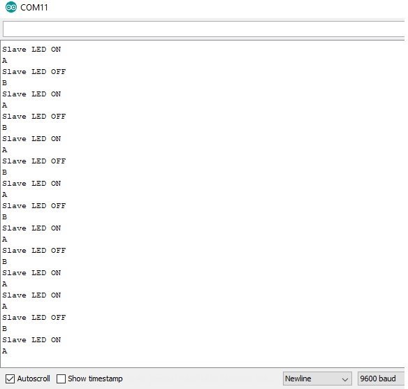
Now upload Arduino code to Arduino Uno and TM4C123 code to Tiva Launchpad using Arduino IDE and Keil uvision respectively.
Now open the Arduino serial monitor. After that click on the reset button of the TM4C123 Tiva launchpad. You will notice that the LED, which is connected with the D7 pin of the Arduino, turns on and off with a one-second delay. Also, you will see the data received from TM4C123 on the serial monitor.
In summary, we learned to use SPI communication modules of TM4C123 to communicate with other SPI based devices.
Video Demo
Conclusion
In conclusion, this tutorial provided a detailed guide on using the SPI communication modules (referred to as SSI in the TM4C123 microcontroller) with the Tiva C Launchpad. We explored how to configure the SPI modules via their registers, emphasizing the versatility of the SSI module, which supports TI serial interface, MICROWIRE, and SPI protocols. By the end of the tutorial, we demonstrated SPI communication between the TM4C123 Tiva Launchpad and an Arduino, showcasing the microcontroller’s ability to interface with other devices effectively. This knowledge enables seamless communication for various embedded applications.
Other TM4C123 Serial Communication Tutorials:
- I2C Communication TM4C123G Tiva C Launchpad
- UART Communication TM4C123
- UART Interrupt TM4C123G Tiva C Launchpad
Other Tutorials:
- PWM TM4C123
- SPI Communication with PIC microcontroller
- UART Communication with Pic Microcontroller
- Use UART Interrupt of Pic Microcontroller
- UART Serial communication with MSP430 microcontroller
Other SPI tutorials:
Hello,
Sir can we transmit data from slave to master in here. Could you make update for this? For example, when tiva sent ‘A’, then arduino answer to tiva ‘done’ after tiva make next process .
hi, I hope you are doing well.
Am working on a project to help me Master SPI communication. am using tm4c123gh6pm MCU with DS1302 module which use SPI protocol.
to configure the RTC module, started by sending 1byte to the control register to disable write protect, then another byte to initialize the seconds register with 30 sec.
using a function that returns uint8_t size , am reading from the seconds register. It’s returning 255 as the result, meaning not responding successfully. I don’t know where am going wrong but would like you assistance.
looking forward to your assistant .You help will be much appreciated ,thank you in advance.
below is my code :
//SPI_init.c
#include “TM4C123.h” // Device header
#include “SPI_init.h”
#include “delay.h”
#include
/*function that initialize spi protocol */
/*pins to be used in ss0
ssi0clk =pA2= clk
ssi0Fss =pA3= CE /RST
ssi0Tx =pA5 = data line
*/
#define CLK 2
#define RST 3
#define TX 5
void SPI_Init(void)
{
SYSCTL->RCGCSSI |= 0x01; /*clock for SSI0 */
SYSCTL->RCGCGPIO |= 0x01; /*clock for port A */
GPIOA->AFSEL |= 0x2C ; /*pA 2,3,5 Alternate function */
GPIOA->PCTL |= 0x00202200 ; /* assign each pin to SSI signals*/
GPIOA->DEN |= 0x2C ; /*digital enable pA2,3,5*/
GPIOA->DATA |= 0x08 ; /*keep CE/RST pin idle HIGH */
//SSI configuration
SSI0->CR1 &= ~0x02 ; /* disable SSI */
SSI0->CR1 |= 0x00 ; /*select SSI as Master*/
SSI0->CC = 0x00 ; /*system clock ssi clock source select */
SSI0->CPSR = 48 ; /*clock prescaler divisor */
SSI0->CR0 |= 10 ; //SCR
SSI0->CR0 |= 0x27 ; /*serial clock rate , clock phase/polarity , protocol mode ,the data size*/
/*MICROWIRE Frame Format */
SSI0->CR1 = 0x02 ; /*enable SSI */
}
void SPI_Write (uint8_t data )
{
//
CE_LOW();// GPIOA->DATA &= ~RST; /*make CE LOW */
while((SSI0->SR & 0x02)== 0 );/*wait untill Transmission FIFO is not full*/
SSI0->DR= data ;/*transmit data over SSI0 TX line */
LED_BLINK(); //blink led after successfull transfer
while(SSI0->SR & 0x10);//== 0);/*wait untill SSI is idle */
CE_HIGH();// GPIOA->DATA = RST; /*make CE pin HIGH when idle */
//
}
void CE_HIGH (void )
{
GPIOA->DATA |= RST;
}
void CE_LOW(void )
{
GPIOA->DATA &= ~RST;
}
uint8_t SPI_READ (uint8_t data)
{
uint8_t Data = 0x00;
//CE_LOW(); /*start reading from slave */
SPI_Write(data);
while((SSI0->SR & 0x08) == 1 );/* wait untill receive FIFO is not full */
Data = SSI0->DR ; // read the received data from the data line
//LED_BLINK();//blink LED after succesfull read from the slave 6
while(SSI0->SR & 0x10);/* wait untill LSB is read */
CE_HIGH();/*CE high after last bit is read */
return Data; //return the received data
}
void LED_BLINK()
{
SYSCTL->RCGCGPIO |= 0x20;
GPIOF->DIR |= 0x04;
GPIOF->DEN |= 0x04;
GPIOF->DATA |= 0x04;
delay_ms(50);
GPIOF->DATA &= ~0x04;
}
and this my main.c
#include “TM4C123.h” // Device header
#include “delay.h”
#include “LCD_display.h”
#include “SPI_init.h”
#include
//macro to define clock Register addresses
#define WR_CREG 0x8E /*control register write*/
#define RD_CREG 0x8F /*control register read*/
#define WR_TCR 0x90 /*trickle charger write register*/
#define RD_TCR 0x91 /*trickle charge register read*/
#define WR_BURST 0xBE /*burst write */
#define RD_BURST 0xBF /*burst read */
#define WR_SEC 0x80 /*Seconds write */
#define RD_SEC 0x81 /*Seconds read */
/*pins to be used in ss0
CLK = pA2
DATA =
RESET =
ssi0clk =pA2= clk
ssi0Fss =pA3= CE /RST
ssi0Tx =pA5 = data line
*/
int main()
{
uint16_t Read_sec ; //keep track of the seconds
char result[20];/*string buffer to store the read */
LCD_init();
LCD_CMD(0x01); /*clear screen */
LCD_CMD(0x80);/*set cursor to line 1 beginning */
delay_ms(500);
string_data(“REAL TIME CLOCK”);
delay_ms(1000);
SPI_Init(); //ninitialize SPI
//LCD_CMD(0x01); /*clear screen */
LCD_CMD(0xC0);/*set cursor to line 1 beginning */
string_data(” Sec “);
delay_ms(500);
/*send control bits , start by sending bit 7 of control register as 0 and also
force the rest to 0this to enable write operation to the rest of the registers*/
SPI_Write(WR_CREG);//go to control register
SPI_Write(0x00);//disable write protect
SPI_READ(RD_CREG);
SPI_Write(WR_TCR); //go to trickle charge register
SPI_Write(0xAB); //enable charger , 2 diodes , 8Kohm
/*write to seconds register
set bit 7 to 0 to start the the clock */
SPI_Write(WR_SEC); //goto seconds control register
SPI_Write(3); //set as 30 seconds
Read_sec = SPI_READ(RD_SEC);
//display on LCD
sprintf(result ,”%d”,Read_sec);
LCD_CMD(0x01); /*clear screen */
LCD_CMD(0x80);/*set cursor to line 1 beginning */
delay_ms(500);
string_data(result);
/* we want to display the time on the LCD thus we use the */
while(1)
{
}
}