2N3819 is a general-purpose N-channel Junction Field Effect Transistor. It operates in depletion-mode and requires reverse biasing to turn off. It is designed for medium to high range frequencies. Furthermore, it has a high gain for wideband frequencies and has an importance in VHF/UHF based systems. It is a small-signal device capable of fast switching, signal amplification, and mixing in low noise applications.
This tutorial will discuss its pinout, configuration, features, specifications, example circuits, 2D model, and its applications.
2N3819 Pinout
Following is the pinout of the 2N3819 N-Channel JFET:

This epitaxial silicon transistor has three pins. The leftmost pin is the source, and the rightmost numbered as 3, is the drain pin. The middle pin serves as the gate of the JFET.
Pin Configuration
The pin configuration detail in tabular is mentioned below:
| Number | Pin Name | Function |
|---|---|---|
| 1 | Source | Source pin |
| 2 | Gate | Gate pin |
| 3 | Drain | Drain pin |
Features and Specifications
- Drain-Source voltage(Vds) : 25Volts
- Drain-Gate voltage(Vdg) : 25Volts
- Gate-Source voltage(Vds) : 25Volts
- Power Dissipation : 350mW
- Drain Current: 100mA
- Gate-Source Cut off voltage (Vds=15 Volts,Ig=10 nA) : -8.0Volts
- Gate-Source Breakdown voltage (Vds=0 Volts,Ig=1.0 uA) : 25 Volts
- Zero Gate Voltage Drain Current (15Volts,Vgs=0Volts) : 2.0 – 20 mA
- Cut off Frequency (Vds=15 Volts,Vgs=0) : 700 MHz
The most important point to note here is that it can provide only 100mA drain current. Therefore, you should it as a switch only when required drain current is less than 100mA.
For more information about the technical details and small-signal characteristics, check the 2N3819 datasheet. The link to the datasheet is provided at the bottom of the article.
2N3819 Alternative Options
- 2N4416
- 2SK162
- 2N5638
- NTE312
Where to use 2N3819?
This N-channel JFET can be used for low side switching only. Because N-channel FETs are used to drive low-side power paths only. But if you want to drive a high-side load, you can use any other P-channel JFET. Another important point here to note here is that the drain current of 2N3819 JFET is 100mA. Hence, it will be used for an application that only requires less than 100mA Drain current.
2N3819 Example Circuits
In this section, circuits based on 2N3819 N-Channel JFET will be discussed.
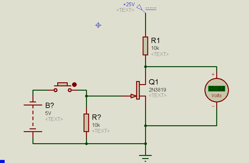
N-Channel JFET as a Switch
The following circuit shows the example of 2N3819 JFET as a switch. A DC voltmeter is connected between Drain and sourcr terminal to measure voltage across Drain terminal.
- When zero voltage is applied to the Gate terminal of N-channel JFET, FET operates in saturation mode and It acts like a closed circuit and almost zero voltage appears across the Drain terminal as you can see on the DC voltmeter.
- Similarly, when enough negative voltage is applied to Gate terminal of N-channel JFET, FET operates in the cut-off region and It acts as an open circuit and input voltage source (+25V) appears across Drain terminal as you can see on the DC voltmeter.
Field Detector Circuit 2N3819
The circuitry for an AC field detector is shown above:
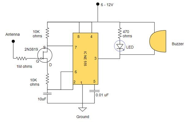
It will explain the working of 2N3819 N-Channel JFET as a field detector. The transistor source terminal is connected with 6-12 Volts of power source to supply voltage to 555 Timer IC. The IC is further connected with an LED, which brightens when the timer turns on, and a buzzer that produces sound whenever a signal is detected. An antenna is connected to the gate of 2N3819 to detect the AC field. Whenever the antenna senses a charge or a wave, it will induce a voltage and pass it to the gate terminal. The change in the gate voltage alters ID and activates the Timer IC. As a result, the led starts to blink, showing the activation of the IC, and the buzzer produces the sound to indicate that a charge is detected by the antenna.
Audio Mixer 2N3819
An audio mixer is a device used to amplify and mix audio signals to produce different sounds and enhance audio quality. The schematic of an audio mixer is as shown :
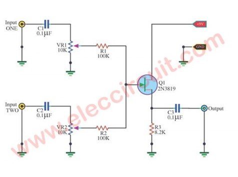
The transistor gate is linked with two audio input channels, followed by coupling capacitors and variable resistors. N-Channel JFETs have high gain. The working of a mixer is similar to that of an amplifier except for the variable resistors’ part. When input signals are applied, gate voltage changes, the drain current changes, which in return varies the voltage drop across the load resistor, performing amplification of the audio signal.
The variable resistors play their role in the mixing of audios. By varying the resistances, we can control the contribution of each input channel in the output mixed and amplified signal. This results in various levels of sounds. The output is coupled with a capacitor so that the resultant signal is a fine quality signal.
Applications
- Low noise applications
- Modulation of signals
- Wideband amplifying systems
- VHF/UHF mixers
- High-Speed Switching Systems
- RF reception and transmission
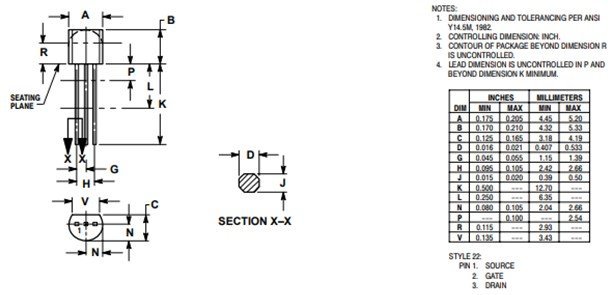
2D Diagram
The following figure shows the 2d model of 2N3819 N-channel JFET. It shows us the physical dimensions of the components needed when a PCB card is designed.
Datasheet
The link to the datasheet is given below to see more details and specifications of the 2N3819 N-channel JFET.
Related Transistors: