2N5089 is an NPN amplifier bipolar junction transistor. It operates as a switch in saturation mode and as an amplifier in the active region. The silicon-based transistor is designed mainly for audio signal amplification to amplify the weak base signal and produce a strong output signal at the collector terminal in low power systems.
This tutorial will discuss its pinout, features, specifications, example circuits,2d model, and applications.
2N5089 Pinout
Following diagram shows the pinout of the 2N5089 Amplifier Transistor:
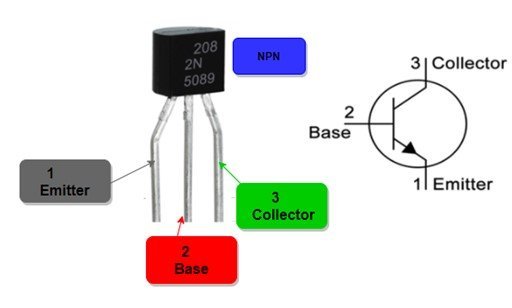
This epitaxial silicon transistor has three pins just like any other NPN BJT transistor has. The leftmost pin numbered as 1 is the emitter terminal, and the rightmost numbered 3 is the collector pin. The middle pin serves as the transistor base, which controls the current flow from emitter to collector.
Pin Configuration
The pin configuration detail in tabular is mentioned below:
| Number | Pin Name | Function |
|---|---|---|
| 1 | Emitter | Emitter pin |
| 2 | Base | Base pin |
| 3 | Collector | Collector pin |
2N5089 Features and Specifications
- Collector-Emitter voltage(VCEO) : 25 Volts
- Collector-Base voltage(VCBO) : 30 Volts
- Emitter-Base voltage(VEBO) : 3.0 Volts
- Power Dissipation (PD) : 625 mW at TA=250C
- Continuous Collector Current (IC) : 50 mA
- DC Current Gain (VCE=5.0 Volts,IC=100 uA) : 400-1200
- CurrentGain BandwidthProduct (VCE=5.0Volts,IC=500uA,f=20MHz) : 50MHz
- Small-Signal Current Gain (VCE=5.0 Volts,IC=1.0 mA,f=1.0 kHz) : 450-1800
For more information about the technical details and noise characteristics, check the 2N5089 datasheet. The link to the datasheet is provided at the bottom of the article.
2N5457 Alternative Options
- MMBT5089 (equivalent)
- MPS650
- MPS6532
- MPSH10
- MPSW0
- ZTX690B
2N5089 Example Circuit
In this section, we will see two example circuits of 2N5089 i.e. as a switch and as an amplifier.
2N5089 as a Switch
Following is a proteus simulation of 2N5089 to control an LED. The two different circuits represent the working of the circuit when the base voltage is the same as the emitter and when the base voltage is greater than the emitter voltage.
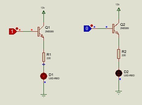
In the first circuit, the collector is provided with a Vcc of 12 volts. The base is connected to a logic toggle. The led is placed at the emitter terminal following 220 ohms of a resistor to limit the excess forward current to avoid led damage. When the logic is turned on, the forward current flows, and the led glows. On the contrary, when the logic is turned off, when voltage is not given to the base terminal, the base potential is the same as the emitter potential, so the led loses its luminosity, as shown by the second circuit.
2N5089 as an Amplifier

Above is the circuitry of 2N5089 as an amplifier. For the amplification of the signal, a common emitter configuration is used. This configuration has a high gain. The base terminal is applied with an input signal, and the collector is provided with some volts to turn on the active mode and operate the transistor as an amplifier. An audio signal is an AC signal. Coupling capacitors are used to avoid the distortion of the signals, which affects the audio quality by displaying high input impedance to low-frequency components.
A capacitor is also placed in series with the output to block the unnecessary DC components at the load/output. RC resistor controls the flow of collector current to control the gain of the amplifier. It is responsible for the frequency response of the circuitry as well. As a result, a small weak radio signal after passing through an NPN amplifier transistor is received as an inverted, amplified radio signal with a high voltage and power gain with fine quality and finds its applications in low noise, audio amplification systems.
Applications
- Switching circuits
- Modulation of signals
- Low noise amplification systems
- High AF systems
- Push-pull circuits
- Temperature sensing systems
2D Diagram
2N5089 comes in two different packaging, i.e., Straight Lead Package and Bent Lead Package. The following figure shows the 2d model of both 2N5089 NPN Amplifier Transistor packages. It shows us the physical dimensions of the components required when a PCB card is designed.

Datasheet
The link to the datasheet is given below to see more details and specifications of the 2N5089 NPN Amplifier Transistor.
Related Transistors:
My opinion for your example “2N5089 as a Switch”. I think it’s worth to mention, don’t use low side LED driver along with a 3.3V powered microcontroller because it’s limiting what type of LED and how many can be driven. Presuming a single InGaN chemistry LED (Green, Blue or White) where the voltage drop is minimum 3.2V for the LED and you need more than 3.9V on the Base (more, because have to add the voltage drop on the 220R resistor).
Calculating even in best case scenario, when voltage drop only 1.7V on LED, 0.7V base-emitter, in this case the achievable maximum LED current is 4mA >>> (3.3V-(1.7+0.7V))/220R=0.004A
Hi bela,
Thanks for your input. We will definitely update the article with your suggestion.
thanks for this post you are providing quality content