2N5457 is a general-purpose N-channel Junction Field Effect Transistor with Drain and Source interchangeable feature. It operates in depletion-mode and requires reverse biasing to turn off. Because depletion types MOSFETs act like a normally closed switch. It has high (AC and DC) input impedance, contrary to other MOSFETs. It is a CMOS technology device used for signal amplification and fast switching in low noise applications.
This tutorial will discuss its pinout, configuration, features, specifications, example circuits, 2D model, and its applications.
2N5457 Pinout Diagram
The following diagram shows the pinout of 2N5457 N-channel JFET.
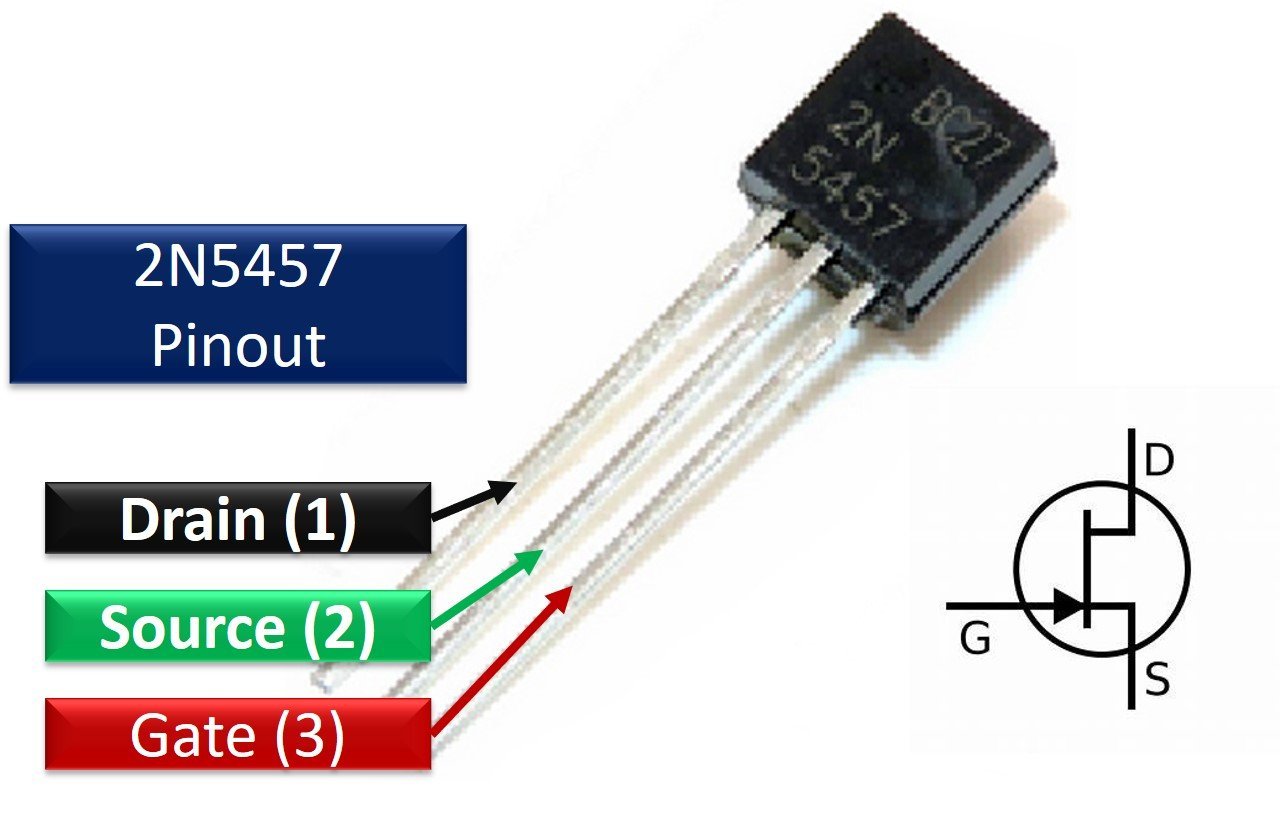
This epitaxial silicon transistor has three pins. The leftmost pin is the drain, and the rightmost numbered as 3, is the gate pin. The middle pin serves as the source of the JFET.
Pin Configuration
The pin configuration detail in tabular is mentioned below:
| Number | Pin Name | Function |
| 1 | Drain | Drain pin |
| 2 | Source | Source pin |
| 3 | Gate | Gate pin |
2N5457 Features and Specifications
- Drain-Source voltage(Vds) : 25Volts
- Drain-Gate voltage(Vdg) : 25Volts
- Gate-Source voltage(Vds) : -25Volts
- Power Dissipation : 310mW
- Gate Current : 10mA
- Gate-Source Cut off voltage(Vds=15Volts,Id=10nA) : -6.0Volts
- Zero Gate Voltage Drain Current(15Volts,Vgs=0Volts) : 5.0mA
For more information about the technical details and small-signal characteristics, check the 2N5457 datasheet. The link to the datasheet is provided at the bottom of the article.
2N5457 Alternative Options
- 2N5458
- J107
- BF246B
- J309
2N5457 Example Circuits
In this section, we will see two example circuit based on 2N5457 N-channel JFET.
2N5457 Switch Circuit
The following schematic diagram shows the use of 2N5457 N-channel JFET circuit as a switch.

N-channel JFET is normally on device. It means at zero gate voltage, it turns on. Moreover, it does not require any biasing voltage for the current to flow from drain to source. It is in its saturation mode. So, when the voltage source is applied to the led and no voltage at the gate terminal of JFET, the led glows. In order to turn off JFET, a sufficient negative voltage should be applied to the gate terminal to make JFET enter the cut off mode. The current wouldn’t flow from drain to source anymore, and the led will lose its luminosity. The resistor used is to limit the current through the led to avoid damage.
You may like to read this:
2N5457 Chopper circuit
The below diagram shows the working of JFET as a chopper.

The drift problem in circuits is due to temperature changes and coupling of direct and alternating current in amplifiers and can be overcome by using choppers.
An input dc voltage is passed through a chopper,, resulting in an alternating signal with the same peak voltage as the input dc signal. It is then amplified using an ac amplifier, and no drift occurs. This amplified ac wave is peak detected to redeem the amplified dc output signal.
A square input signal is applied to the gate terminal to make it operate as a chopper. It alternates the JFET between saturation mode and cut off mode.
Just like input dc voltage, input ac voltatransistor’s ge can also be amplified without any drift. A low ac input signal is applied at the chopper. The resultant wave is then amplified through an ac amplifier and gets rid of the drift. The amplified wave is then peak detected to redeem the original low input ac signal applied to the chopper.
Applications
- Low noise applications
- Modulation of signals
- Low noise amplifiers
- Current limiting systems
- Phase-shifting Oscillators
2d Diagram
The following figure shows the 2d model of 2N5257 N-channel JFET. It shows us the physical dimensions of the components needed when a PCB card is designed.

Datasheet
The link to the datasheet is provided here to view further features and specifications of 2N5257 N-channel JFETw.
Related Electronics Components:
In the intro, it is mentionned that this transistor is based on CMOS technology, but as I am used to, CMOS technology is the combination of a PMOS and NMOS, and would also imply a Metal Oxyde insulation between the Gate and the Canal. Is it a typo or is it another use of the acronym CMOS, a use that I am not aware of ?
Please check here: https://en.wikipedia.org/wiki/JFET