74HC157 is a high-speed multiplexer integrated circuit consisting of four 2-inputs digital multiplexers inside the chip. It is pin-compatible with Low-power Schottky TTL. It has two control inputs namely enable and select input. Additionally, it has two groups of registers. The select input determines the register from which the data comes. Its operation is specified over a temperature range of -55 °C to 125 °C.
Recommended Components
The following parts are used in this article, along with a generic electronics kit that is handy for building and testing the circuit.
| Component | How it’s used | Buy on Amazon |
|---|---|---|
| 74HC157 quad 2:1 multiplexer | The 74HC157 quad 2-input multiplexer this article covers. | Check Price |
| Electronic component assortment kit (1390 pcs) | A handy assortment of resistors, capacitors, LEDs, diodes and transistors for building circuits. | Check Price |
| Digital multimeter (AstroAI) | Measures voltage, current, resistance and checks continuity while you build and debug. | Check Price |
| Breadboard | Solderless base for prototyping the circuit. | Check Price |
| Jumper Wires | Make the connections on the breadboard. | Check Price |
As an Amazon Associate we earn from qualifying purchases. Prices and availability are accurate as of the date/time indicated and are subject to change.
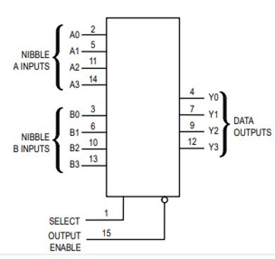
74HC157 Pinout Diagram
As you can see from the pinout diagram that it has four multiplexer channels. To differentiate between them, we give different colors to multiplexer channels. It is having 16 pins. Each mux powers with a common power supply.

Pin Configuration Description
74HC157 IC Pin Configuration details are given below.
Pin#01: SELECT
It is an enable select pin which is used to select the input lines from which the data is presented at the outputs.
Pin#02, 05, 11, 14
These pins are the input A of the four 2:1 multiplexers.
Pin#03, 06, 10, 13
These pins are the input B of the four 2:1 multiplexers.
Pin#04, 07, 09, 12
These are the output pins of multiplexers.
Pin#08: GND
It is connected to the ground of the circuit.
Pin#15: ~STROBE
This input is active low and is responsible for enabling or disabling outputs.
Pin#16: Vcc
This is the positive power supply.
74HC157 Features
The few main specifications of this IC are:
- Quad multiplexer IC with a voltage range of 2V to 6V.
- Displays outputs in the non-inverted form.
- It has buffered inputs and outputs.
- Capability of driving 10 LS-TTL loads.
- The input voltage range is 1.35V to 3.15V.
- The outputs are directly Interfaced to CMOS, NMOS, and TTL.
- It is compatible with TTL/CMOS Input Logic.
- The maximum propagation delay is 25ns at Vcc = 4.5V.
Alternative Multiplexers
- CD4052
- SN74LS153
- 74LV4053
- CD4053
- MPC507AU
Where to use it?
A multiplexer is a digital electronics device having two or more input and one output. It always has a select pin that selects the input that should appear on the output pin. The size of the select pins depends on the width of the mux. This Mux IC consists of quad 2×1 multiplexers within a single chip. It is also known as a quad multiplexer IC. For a 2×1 size mux, a one-bit select line is enough. Because it selects from two inputs only.
Although it has four mux, but we cannot control each mux individually. Because a common select line controls all muxes. Therefore, if you are looking for more than one 2×1 mux inside a single chip and want to control each mux with a single select line, this is the best choice for you.
74HC157 IC is intended for use in multiplexing of data or in communication lines. It has four multiplexers consisting of two input pins. You can use this IC in arithmetic logic units of computer memory. It can also be used to implement Boolean functions.
How to use 74HC157 Quad Mux?
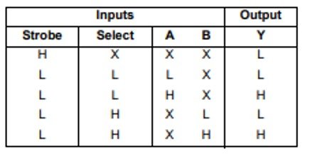
It has a select control input pin which selects whether the input data from nibble A or nibble B inputs will be displayed at outputs in non-inverted form. A low signal applied at this input will select the A inputs and B inputs are selected on applying high signal at this input. Pin 15 is an enable output pin. When it is applied with a High logic level, it disables all the four data outputs. The outputs will not change no matter whatever input is applied.
- In this Proteus simulation, we use only one 2×1 multiplexer.
- As you can see, the input reflects on the output pin according to the value of the select line.

Internal Logic Diagram
The logic diagram of this IC is given below. For normal operation, it is grounded or applied with a low voltage signal. Power the IC with a voltage supply in a range of 2V to 6V. The logic equations for all the four outputs are:
Y1 = E ´ (B0 ´ S + A0 ´ S)
Y2 = E ´ (B1 ´ S + A1´ S)
Y3 = E ´ (B2 ´ S + A2 ´ S)
Y4 = E ´ (B3 ´ S + A3 ´ S)
2×1 Mux Truth Table
The truth table is given to indicate the effect of inputs on output behavior.
Example Circuit

The example circuit of this IC is a water level indicator. This IC is used to detect whether the water tank is empty or not. When the tank is empty, all the outputs of multiplexer IC are high. When the tank is full, all the outputs will become low indicating that the tank is filled. You can connect the outputs of 74HC157 with the inputs of CD4511 which is used to detect the level of water. Connect a 7-segment display which will indicate the level of water.
Applications
Multiplexers are used in numerous applications. The 74HC157 is also a multiplexer IC. Its applications are as follows:
- Computer memory
- Arithmetic logic units
- Network lines
- Telephone line selector
- Communication systems
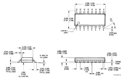
74HC157 2D Diagram
The two-dimensional diagram of its 16 pin SOIC package is given.