74LS00 is one of the famous and most basic gates from a family of logic gates. There are three kinds of gates, AND, OR and NOT. All three gates come up with different internal circuit and they have different uses in every device. By combining these three circuits we can make some other gates which are NAND, NOR, XOR, and XNOR. All of these gates can be made easily using transistors, resistors, and capacitors. When we make these circuits then the size of a single gate becomes larger than our expectations.
So, there are multiple kinds of ICs that come with internal gates in a small size package. Here we will discuss and IC called 74LS00 which is also known as IC 7400. 74LS00 is NAND gates-based IC. It has 14 pins which all connected with 4 NAND gates. Due to the NAND gate known as universal gate, 74LS00 can be converted into OR and NOT gate easily. The IC comes in three packages, SOIC, PDIP, and SOP.
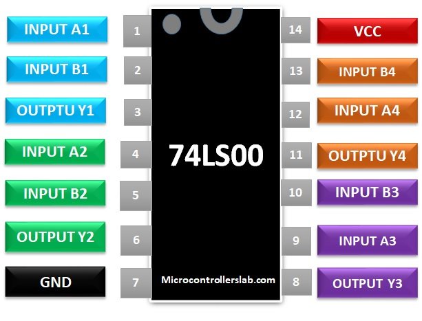
74LS00 Pinout
Note: Other CMOS based NAND gate CD4011
74LS00 NAND Gate PIN CONFIGURATION
| PINS | DETA | |
|---|---|---|
| A1 | Pin 1 | Pin 1 will be the input of the first NAND gate in IC 74LS00. |
| B1 | Pin 2 | Pin 2 will be used as the second Input of First NAND gate. |
| Y1 | Pin 3 | The output of the first NAND gate will be available at Pin 3. |
| A2 | Pin 4 | Pin 4 will be used for the input of the second NAND gate. |
| B2 | Pin 5 | The second input of the second NAND gate will be given at Pin 5. |
| Y2 | Pin 6 | The output of the second NAND gate will be available at Pin 6. |
| GND | Pin 7 | Pin 7 will be used at the common ground by devices and the power supply that will use with 74LS00. |
| Y3 | Pin 8 | Third NAND gate output will be at Pin 8. |
| A3 | Pin 9 | Pin 9 will be used as the first input pin for the third NAND gate. |
| B3 | Pin 10 | Pin 10 will be the second input of the third NAND gate. |
| Y4 | Pin 11 | The output of the fourth NAND gate will available at Pin 11. |
| A4 | Pin 12 | Pin 12 will be used for the first input of the 4th NAND gate. |
| B4 | Pin 13 | The second input of the fourth NAND gate will be at Pin 13. |
| Vcc | Pin 14 | Pin 14 will be used to give power to the IC. |
74LS00 FEATURES
- This IC can be used as a NAND gate however due to the universality of the NAND gate, it can be converted into other gates easily.
- The internal structure of IC is TTL based that’s why its output also comes in TTL.
- It comes in multiple packages, SOIC, PDIP and SOP.
- It can be used in HIGH-frequency systems.
SPECIFICATIONS
- The operating voltage of 74LS00 is 4.75 to 5.25.
- The maximum power supply voltage could be at 7V but in case of a minor increase in voltages above 7V, the IC could burn easily.
- Maximum current draw from each gate at the output will be 8mA.
- IC has a maximum ESD of about 3.5KV.
- The IC has a typical rise and fall time is 15ns.
- IC has a maximum operating temperature is about 0 – 75 degrees.
- The Low-level input voltage at the gate will be 0.8 and the HIGH level will be 2V.
- IC has an internal clamp voltage of about -1.5V.
For more information check the datasheet.
RELIABILITY
- 74LS00 is one of the cheapest IC that makes it more popular than the other ICs.
- It could perform HIGH NAND speed operation within nanoseconds without any use of a microcontroller or processor.
- The IC has four NAND gates that can be used further for any other gate separately.
- 74LS00 can be used as an inverter because the NAND gate can be used to make a NOT gate just by reconfiguring the pins.
74LS00 2 input NAND Gate WORKING
The IC comes up with four NAND gates but when each NAND gate comes up with two types of internal structure. The first one is CMOS and the second one is PMOS. The structure may look different when we see it but its main function is the same. The CMOS NAND gate comes up with four transistors. The combination of transistors and power supply make a little complex circuit, which gives the HIGH and LOW state on different input combinations. Here’s the internal structure of the NAND gate.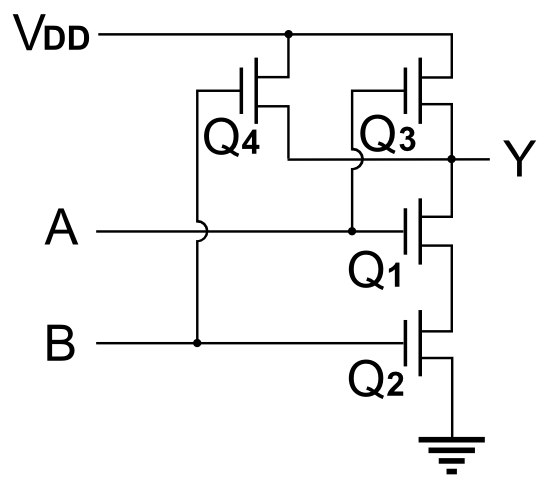
In structure the VDD will be used as the Power input and A, B will be used as Logic inputs. The Output will be given at Y. Here Q1, Q2, Q3 and Q4 will represent the transistors. When Input single will be HIGH then the output should be HIGH at the output with respect to Q1 and Q2 transistor, but the output will be LOW due to the further two transistors Q3 and Q4 the output will be inverted every time. This combination of 4 transistors makes the circuit of the NAND gate. The output in logic gates is always dependent on the input. So, every NAND gate in this IC will follow the following table in case of different inputs.
| INPUT | OUTPUT | |
|---|---|---|
| A | B | Y |
| 0 | 0 | 1 |
| 0 | 1 | 1 |
| 1 | 0 | 1 |
| 1 | 1 | 0 |
You may notice that when input on the NAND gate will be HIGH then there will be LOW state on the output otherwise there will be HIGH state on output no matter the input states are.
Examples with 74LS00 NAND Gate IC
Below are the three examples that are designed using a 74LS00 8-bit 2 input quad NAND gate IC.
NAND gate is a universal gate that can be converted to other gates easily. To convert the NAND gate to OR, NOT or even AND gate we just need to follow some combinations. These combinations will be different for each and every gate. First, we will convert the NAND gate to NOT gate. To convert the NAND gate to NOT gate we will need to combine its first two input wires. Then we will need to apply the input on that single input pin which will make the whole gate into NAND gate. Here the representation.
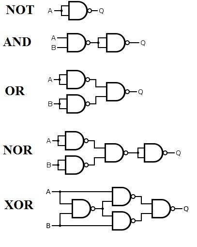
To convert the NAND gate to OR gate we will need to add the two Not gates at the input pins. To attach the NOT gates we could use the NOT gate made from NAND gate as we discussed above. Now to convert the AND gate from NAND gate we can use the NOT gate at the output pins to make it AND gate easily. We can make other XOR and XNOR gate from the NAND gate too but that will require all four gates of 74LS00. Here is the graphical representation of these gates.
EXAMPLE in proteus
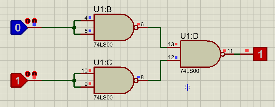
In proteus, we will use the IC just for normal function. We will convert all four gates into other gates. Like one NAND gate will be in NOT and others will be in OR gate. To do this first insert the IC and then some logic state inputs and viewers. After that just make the first 3 NAND gates into not gates by combining their inputs pins. Then attach the output of two NAND gates with the input of four NAND gates. Now give the input on the first gate, you will get the inverted outputs.
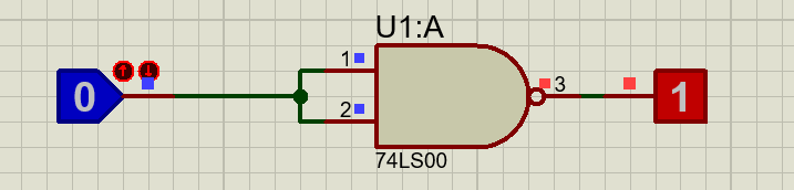
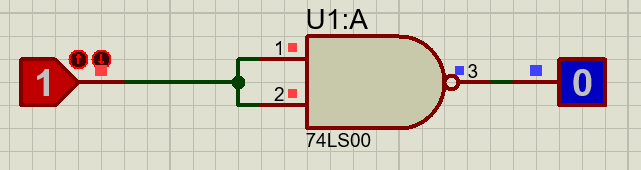
Now apply the logic on the other circuit the result will be the same as we expected.
The usage of the IC is very simple. Due to its wide usage, it can be found easily. The only protection we should worry during using the IC is about voltage. Only high voltages can affect the IC. Here we only use the IC to make two kinds of gates. You can use it for further designing.
74LS00 APPLICATIONS
- It can be used in general-purpose logic.
- Most of the digital electronics use 74LS00 due to its low cost.
- PCS and some Notebooks also comes up with NAND gates IC.
- The server has wide use of 74LS00.
- IC 74LS00 also many usages in ALU and other digital Systems.
- In networking systems, LS7400 is also used for logic states.
The representative circuit is incorrect. The 54/74LSXXXX family is so named because it uses Low-power Schottky transistors, but your representative circuit uses MOSFET devices. Your representative circuit is fine from a logic perspective, but oftentimes we need to know the input and output structures to determine bias requirements as well as fan-in and fan-out.