74LS08 is a Quadruple 8-bit Two Input AND IC. Gate AND gate is a digital circuit used to convert the logic state to a specific logic. In AND gate two logics state signals are used. The first one is HIGH, which is also known as 3-5Volts and the second one is LOW which is represented by 0-2.6Volts. A single AND gate uses two input pins and one output pin. The output will also be in the HIGH and LOW state, but it will only HIGH when both input states will be HIGH. The single AND gate can be made easily by using transistors and resistors or diodes.
Introduction to 74LS08
The single AND gate circuit made manually always has large size, to solve this issue an IC name 74LS08 can be used as an AND gate. This IC comes with four AND gates. Every AND gate can be used separately without affecting the others. IC 74LS08 uses only one single power supply and it also comes in multiple packages to solve the requirement according to the circuit. The output of the IC always comes in TTL which makes it easy to work with other TTL devices and microcontrollers. The IC 74LS08 is smaller in size and it has a much faster speed which makes it reliable in every kind of device.
Other logical gates ICs of the same series are: 74LS73, 74LS00, 74LS02, 74LS04, 74LS138
Pin Diagram 74LS08
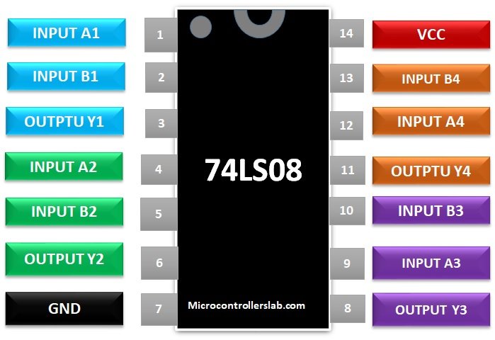
74LS08 – Quadruple AND Gate Pinout Details
| PINS | DETAILS | |
|---|---|---|
| A1 | Pin 1 | Pin 1 will be used as the first input pin for the first AND gate in IC 74LS08. |
| B1 | Pin 2 | Pin 2 will be used for second input pin for first AND gate in IC 74LS08. |
| Y1 | Pin 3 | The output of the first AND gate will be received at Pin 3. |
| A2 | Pin 4 | Pin 4 will be used for the first input pin of second AND gate in IC 74LS08. |
| B2 | Pin 5 | Pin 5 will be used to give the second input to the second AND gate in IC 74LS08. |
| Y2 | Pin 6 | Pin 6 will be used to receive the output of second AND gate from IC. |
| GND | Pin 7 | Pin 7 is a ground pin; it will be used as common ground by other communication devices with IC and Power Supply. |
| Y3 | Pin 8 | Pin 8 will be used to receive the output of third AND gate from the IC. |
| A3 | Pin 9 | Pin 9 will be used to give the first input to the third AND gate to the IC. |
| B3 | Pin 10 | Pin 10 will be used to give the second input to the third AND gate to the IC. |
| Y4 | Pin 11 | Pin 11 will be used to receive the output of fourth AND gate from the IC. |
| A4 | Pin 12 | Pin 12 will be used as the first input pin of forth AND gate. |
| B4 | Pin 13 | Pin 13 will be used as the second input pin of forth AND gate. |
| VCC | Pin 14 | The Power Supply will be provided at pin 14 to make the IC functional. |
Quadruple Two Input AND Gate Features
- The IC has low power consumption.
- IC 74LS08 has a much fast operating speed.
- It comes in multiple packages, SOIC, PDIP, and SOP.
- It is much cheaper and easy to operate.
- Its output comes in TTL, which makes it operate able with most of the devices and microcontrollers.
- A single AND gate can be used without affecting the other ones.
- A single power supply can turn all four gates.
SPECIFICATIONS 74L08
- The operating voltage range of IC is 4.75 – 5.25 Volts. The voltage recommended for IC should be 5 volts but IC can hold up to 7 volts maximum.
- The IC gives 8mA maximum current at its outputs.
- IC 74LS08 has 18ns Rise and Fall time.
- It can operate in the temperature range from 0 to 70 degree but it also has the ability to store the temperature of -65 to 150 degrees.
RELIABILITY
- A single IC gives four AND gates.
- The IC cost much less the single handmade AND gate.
- The IC is smaller in size and comes in multiple packages which make it reliable for any small size devices.
- 74LS08 can be operated with any TTL device without using any device as an interface.
How to use a 74LS08 IC
To understand the IC, we should understand how a single AND gate works. The AND gate has three types of combinations and every combination has the same outputs on specific inputs. We will use here transistor-based AND gate. In transistor-based AND gate the basic circuit consisting of two transistors which are used as a switch to change the state on output on different inputs.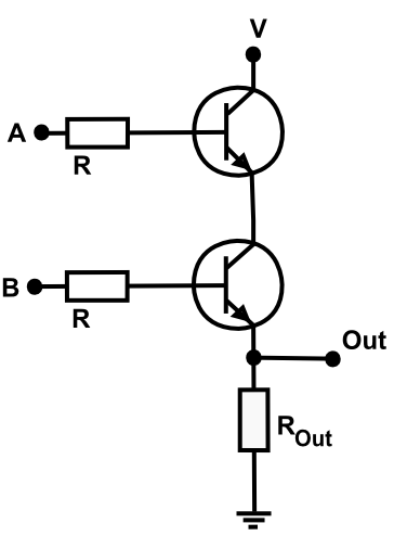
In IC 74LS08 both transistors will be connected in series. The power will be connected with the collector of the first transistor and output will be received on the emitter of the second transistor. The two inputs will be given to the base of both transistors. The inputs will let the current flow from the transistors. When the Input signal will be HIGH on both inputs then current could flow through the transistors and full voltages will be received on the output pin.
In other cases, if only one pin will be LOW in the circuit then the output will be LOW because there is no flow of current from the transistors. No matter which type of AND gate we use the output will always the according to the following table which is known as a truth table.
| INPUTS | OUTPUTS | |
|---|---|---|
| A | B | |
| 0 | 0 | 0 |
| 0 | 1 | 0 |
| 1 | 0 | 0 |
| 1 | 1 | 1 |
A single or combination of two AND gates cannot be used to make any other gate but AND gate can be used to design other gates. Like using one NOT gate AND gate can be converted into NAND gate. AND gate can be used to design other gates too like XOR and XNOR, but to design like other gates it needs to be used with NOT and OR gate. Here’s the design for those gates which are designed with the help of AND gate.
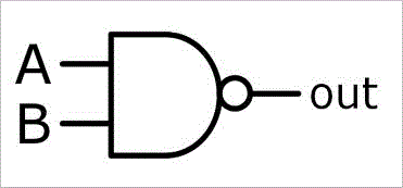
Figure 1: NAND gate
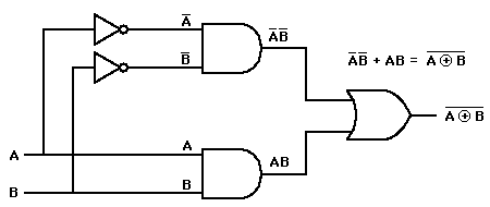
Figure 2: XNOR GATE

Figure 3: XOR GATE
Where to use 74LS08 IC?
As we know that AND gate cannot be used to design any other gates. So here we will only use the one AND gate of IC will verify the truth table. First, take the IC 74LS08 in proteus the attach it to the logic gates. The apply each and every logic. First, apply both inputs LOW. You may notice that OUTPUT is LOW which is according to the truth table.

Figure 4: ALL LOW
The apply one logic HIGH and other one LOW. First Apply first input pin HIGH, you may notice that the output is still zero which is according to the truth table too. Then change the state for the first pin to LOW and second to HIGH the output will still be LOW.
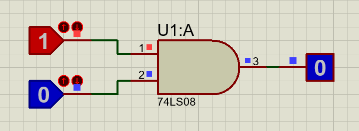
Figure 5: FIRST HIGH
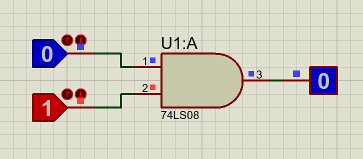
Figure 6: SECOND HIGH
NOW apply both inputs HIGH. In the case of both inputs HIGH the output will HIGH too., which proves the truth tables.
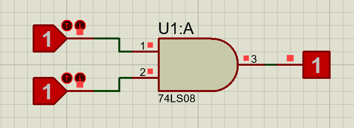
Figure 7: ALL ONE
The AND gate is reliable to use in that logic where output should be HIGH when all the conditions should be met. If any single condition is false or LOW then the circuit should not work. The IC 74LS08 help us to solve the issue of NAND gate in many cases due to its reliability and size too.
APPLICATIONS 74LS08
- 74LS08 IC used to perform general-purpose logic of AND gates.
- It is also used in the following devices
- Digital Electronics
- Networking Devices
- Servers
- Memory Units
- ALU
- The IC has wide use in multiple Digital Systems.