74LS138 is a complex TTL based logical device used to convert 3-bit binary data to 8-bits. The actual purpose of this chip is designed for demultiplexing or in machine language we can say as a decoding device. The device takes 3 input data and converts it to 8-bit data. This chip is high used in decoding in memory to minimize the effect of decoding. The chip includes three enable pin, three input pins, and 8 output pins.
Introduction to 74LS138
The three enable pins comes up as control pins that minimize the use of external gate and inverter when data is expanding. The IC could use as decode without any external inverter for multiple lines. In the case of the 32-line decoder IC will require one inverter. 74LS138 uses enable pins as data input to the input decoder, without enabling pins active the data won’t be able to decode. 74LS138 is designed with Schottky diodes which helps to suppress line-rigging and it makes the design simple.
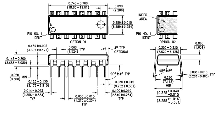
Pinout of 74LS138 decoder

PIN CONFIGURATION
| `PINS | DETAIL | |
|---|---|---|
| A | Pin 1 | Pin no 1,2,3 will be used as input pins. The data on input pins could be any value in bits. The value on these pins will affect the output value. |
| B | Pin 2 | |
| C | Pin 3 | |
| G2’A | Pin 4 | Pin 4 is the first enable pin of the decoder. It will affect the output very much. Pin 4 is an active low state pin. In case of HIGH of state of pin 4, the other enables and input condition won’t be matter, because then there will be no effect on output. |
| G2’B | Pin 5 | Pin 5 is the second enable pin of the decoder. It will affect the output as much as other enable pins. Pin 4 is an active low state pin. In case of HIGH state on pin 5, the other enables and input condition won’t be matter, because then there will be no effect on output just like other enable pins. |
| G1 | Pin 6 | Pin 6 is the third enable pin of the decoder. It will affect the output as much as other enable pins. Pin 6 is an active HIGH state pin. In case of LOW state on pin 6, the other enables and input condition won’t be matter, because then there will be no effect on output. |
| GND | Pin 7 | Pin 7 will be used as ground common for devices connected to the decoder. |
| Y7 | Pin 8 | There are total 8 outputs on 74LS138 and all pins from 8 – 15 will represent the out of the decoder. These pins will give the output state as an active LOW. |
| Y6 | Pin 9 | |
| Y5 | Pin 10 | |
| Y4 | Pin 11 | |
| Y3 | Pin 12 | |
| Y2 | Pin 13 | |
| Y1 | Pin 14 | |
| Y0 | Pin 15 | |
| Vcc | Pin 16 | Pin 16 will be used to power up the IC. |
74LS138 FEATURES
- IC 74LS138 is designed especially for some high-speed works like memory decoders and data transmission systems.
- It comes up with three enable pins that simplifies the device for inputs from cascading and data reception problems.
- It is designed with Schottky clamped diodes for High performance.
- IC 74LS138 has internal ESD Protection.
- It comes in multiple packages, Such as SOIC, PDIP & SOP.
- The inputs on the decoder can be higher than the Power supply voltages.
- It can be used in any environment due to its high operating temperature.
SPECIFICATIONS 74LS138
- The power input range for the decoder is 1.0 – 5.0 Volts.
- The Typical Propagation time for IC is 21ns
- Its Low Power Consumption is almost 32mW
- The decoder can work in the temperature range from -40 to +125 degree.
Other Decoders: 74LS48, 74LS145, CD4052
74LS138 decoder WORKING
The IC has a little complex circuit. IT comes up with two inverters an input pins and two inverters at two enable pins. The three enable pins to pass through the AND gate and control the outputs. The output came out through NAND gates. Every output automatically inverted by not gate of NAND gate. All NAND gates on output are controlled by enabling pins directly let the output only when two enable pins E1’ and E0’ is LOW and E2 is HIGH. If all enable pins are active then there will be output, it doesn’t matter input is HIGH or LOW. In case of any single enable pin is not active then there won’t be any output, it doesn’t matter what the inputs and other enable pins are.
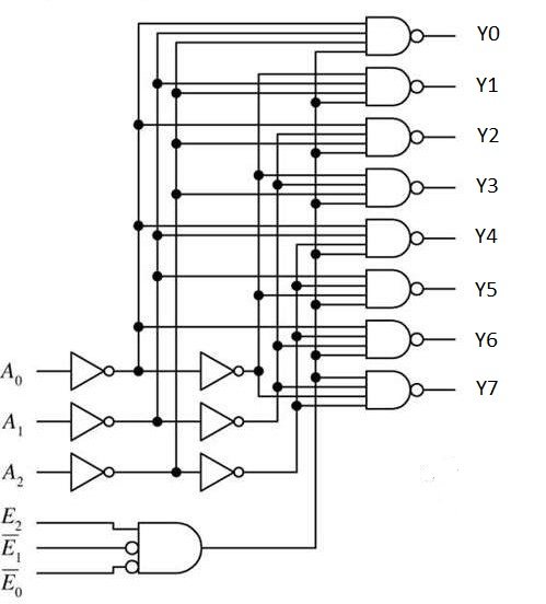
Every single output has a fixed input state. There are three input states and all three inputs which make total of 8 outputs. Every input makes the one output state LOW when enable pins are active. The output and input will be depending on the following truth table.
74LS138 Truth Table
| ENABLES | INPUTS | OUTPUTS | |||||||||||
|---|---|---|---|---|---|---|---|---|---|---|---|---|---|
| E0’ | E1’ | E2 | A2 | A2 | A0 | Y7 | Y6 | Y5 | Y4 | Y3 | Y2 | Y1 | Y0 |
| 1 | X | X | X | X | X | 1 | 1 | 1 | 1 | 1 | 1 | 1 | 1 |
| X | 1 | X | X | X | X | 1 | 1 | 1 | 1 | 1 | 1 | 1 | 1 |
| X | X | 0 | X | X | X | 1 | 1 | 1 | 1 | 1 | 1 | 1 | 1 |
| 0 | 0 | 1 | 0 | 0 | 0 | 1 | 1 | 1 | 1 | 1 | 1 | 1 | 0 |
| 0 | 0 | 1 | 0 | 0 | 1 | 1 | 1 | 1 | 1 | 1 | 1 | 0 | 1 |
| 0 | 0 | 1 | 0 | 1 | 0 | 1 | 1 | 1 | 1 | 1 | 0 | 1 | 1 |
| 0 | 0 | 1 | 0 | 1 | 1 | 1 | 1 | 1 | 1 | 0 | 1 | 1 | 1 |
| 0 | 0 | 1 | 1 | 0 | 0 | 1 | 1 | 1 | 0 | 1 | 1 | 1 | 1 |
| 0 | 0 | 1 | 1 | 0 | 1 | 1 | 1 | 0 | 1 | 1 | 1 | 1 | 1 |
| 0 | 0 | 1 | 1 | 1 | 0 | 1 | 0 | 1 | 1 | 1 | 1 | 1 | 1 |
| 0 | 0 | 1 | 1 | 1 | 1 | 0 | 1 | 1 | 1 | 1 | 1 | 1 | 1 |
In truth table “X” represent the don’t care, it is due to the conditions we face in enable pins as we discussed above. The 74LS138 is the fastest memory and system decoder. It has wide use in our multiple applications.
74LS138 3-8 decoder APPLICATIONS
- It is widely used in line decoders.
- Servers also come up with 74LS138.
- Some digital systems like microcontrollers still use 74LS138 for data decoding.
- Telecom and memory circuits also use decoder due to the limited number of the data line.
Proteus Simulation Example
The de-multiplexer 74LS138 can work with any microcontroller or TTL device. It will just need HIGH and LOW inputs states to work. Now we will use the decoder in Proteus with logic gates to understand its functionality according to the truth table. Add the logic states to enable and input pins, also add the logic viewer. First, give the all input zero but enable on the active state. You will notice in the below image that there will be output at Y0.

The E1, E2 and E3 are on the active state but the inputs are at a LOW state, but we are still getting the output at input LOW state. Now change one of the enable pin to inactive. You will notice that there will be no output when inputs are even at a HIGH state.

The minimum input is 000 and the maximum input is 111. At minimum input, the out will be 0 at Y0 and at maximum input, the output will be 0 at Y7. The effect of input will be very quickly on output only on the enable state. 74LS138 is a 3 to 8-bit demultiplexer but there is also some demultiplexer more than 3-bit input. In that case, to find out their no of output we use the following formula 2n. In this formula, the n is representing the no of inputs. The total no of inputs will decide the total no of outputs for all kind of de-multiplexer.