74LS76 comes with dual JK flip flops. JK flip flops are widely used in daily electronics devices by many methods but the basic operation of the JK flip flop is to store a bit. JK flip flop allows to store a bit and then allows it to use for further functions. in digital electronics circuits. JK flip flop is one of the popular flip flops due to its clock input, pre-set, and clear functionalities. The JK flip-flop changes its state under the clock pulse signal. The clock signal can be either a positive edge or a negative edge. The clock pulse gives multiple advantages to the flip flop. 74LS76 also has provided a feature to neglect or prevent invalid outputs.
74LS76 Introduction
JK flip flops can be designed by manually using simple gates but to avoid circuit complexity the 74LS76 gives the advantages to use two JK flip flops at the same time. The JK flip flop in this 7476 IC also has a preset and clear function which allows the IC to bypass the clock and inputs and give the different outputs. 7476 is TTL based and can be operated with any TTL based device or any microcontroller. The IC comes in multiple packages that make the IC use any hardware according to the requirement. The multiple IC can be used to make further ICs in case of necessary.
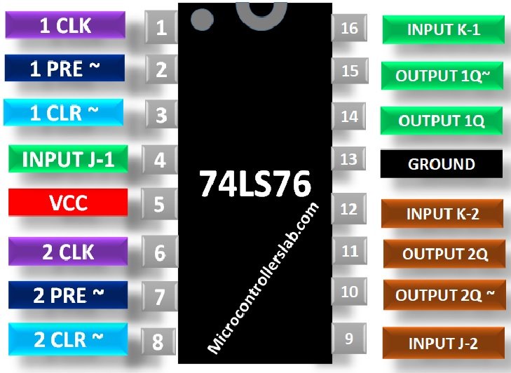
74LS76 Pinout Diagram
| PINS | DETAIL | |
|---|---|---|
| 1 CLK | Pin 1 | Pin 1 is an input pin. It is used to give the clock pulse to the first JK flip flop. HIGH to LOW pulse will only affect the flip flop. |
| 1 PRE’ | Pin 2 | Pin 2 is a preset input pin. It is used to make the output (1Q) of first flip flop HIGH. It’s an active LOW pin. |
| 1 CLR’ | Pin 3 | Pin 3 is a clear input pin of the first flip flop. It is used to reset the output of first flip flop. It’s an active LOW pin. |
| Input 1, J | Pin 4 | Pin 4 is the first input pin of the first flip flop. It is used to give the first input data bit to the IC. It can be HIGH or LOW. |
| VCC | Pin 5 | Pin 5 is used as the power pin. It is used to power up the IC to make it functional. |
| 2 CLK | Pin 6 | Pin 6 is an input pin. It is used to give the clock pulse to the clock of the second JK flip flop. HIGH to LOW pulse will only affect the IC. |
| 2 PRE’ | Pin 7 | Pin 7 is a preset input pin of the second flip flop. It is used to make the output (2Q) of second flip flop HIGH. It’s an active LOW pin. |
| 2 CLR’ | Pin 8 | Pin 8 is a clear input pin of the second flip flop. It is used to reset the output of second flip flop. It’s an active LOW pin. |
| Input 2, J | Pin 9 | Pin 9 is the first input pin of the second flip flop. It is used to give the first input data bit to the IC. It can be HIGH or LOW. |
| 2Q’ | Pin 10 | Pin 10 is the second output pin of the second flip flop. It will give the inverted output of Pin 11. |
| OUTPUT 2Q | Pin 11 | Pin 11 is the first output pin of the second first flop. It will give the output bit of the second flip flop. |
| Input 2K | Pin 12 | Pin 12 is the second input pin of the second flip flop. It is used to give the second input data bit to the IC. It can be HIGH or LOW. |
| GND | Pin 13 | Pin 13 is a ground pin. It is used to make common ground with power supply and other devices if there’s any. |
| 1Q’ | Pin 14 | Pin 14 is the second output pin of the first flip flop. It will give the inverted output of Pin 15. |
| OUTPUT 1Q | Pin 15 | Pin 15 is the first output pin of the first flip flop. It will give the output bit of the first flip flop. |
| Input 1K | Pin 16 | Pin 16 is the second input pin of the first flip flop. It is used to give the second input data bit to the IC. It can be HIGH or LOW. |
Other equivalent FF are: 74LS73, 74LS76A
Also if you want alternatives of this IC: 74LS107, 4027B, HEF4013, CD4042
How JK Flip-Flop Works?
74LS76 has 5 input pins and two output pins. The output will be depending on almost every input pin. When IC has a LOW state at reset pin then the output pin will be LOW and at the inverted output, the state will be HIGH. Now the other input pin knows as preset. When preset will be at HIGH state then the output pin will be HIGH and at the inverted output, the state will LOW. To use the IC we need to keep these will LOW, in case of HIGH state on both pins both output and inverted output will give HIGH state. The reset pin and clear will have these states at different inputs.
| INPUTS | OUTPUTS | ||
|---|---|---|---|
| CLEAR | PRESET | Output | Inverted Output |
| 0 | 0 | 1 | 1 |
| 0 | 1 | 0 | 1 |
| 1 | 0 | 1 | 0 |
| 1 | 1 | DEPENDS ON OTHER INPUT PINS |
When clear = 1 and preset = 1 then the output will be change on the HIGH to LOW clock pulse depending on the J and K input. When J and K both inputs will be LOW then there won’t be any change in output. The output will be depending on the previous state. In the case of J = 1 and K = 1, the output will be kept toggling at each clock pulse. The other states will be according to the following truth table.
| CLOCK | INPUTS | OUTPUTS | ||
|---|---|---|---|---|
| J | K | Q | Q’ | |
| H – L | 0 | 0 | Q | Q’ |
| H – L | 0 | 1 | 0 | 1 |
| H – L | 1 | 0 | 1 | 0 |
| H – L | 1 | 1 | TOGGLE OUTPUT |
The above two tables explain the general working of JK FF, this truth table depicts the functionality of 74LS76 with clear and preset features.

0-9 Counter Example with 74LS76
In this example, we are going to build a 3-bit counter using JK flip flop and then we will show the value by converting it to decimal on the 7-segment. To design a three-bit counter we will need an extra component which is AND gate and then we will use four JK flip flops. After designing the bit counter, we will use the IC 74LS76 to convert the binary data to common cathode 7-segment. The clock pulse will generate the output and IC will show the data on the 7-segment. Here’s the image.

In three bits of data, we can store 000 to 111 data which is eight values. And 7 segments are showing value from 0 to 7 in decimal. The JK flip flop storing each and every value and generating the new values on each clock pulse. 74LS48 is used as a BCD to 7-segment decoder. We can receive the value any time before the clock pulse changes. In microprocessors and controller, the clock pins are controlled by manual signals to replace the data until then the data remains store and this process makes the flip flop best for temporary data storage in multiple devices.
Proteus Simulation
74LS76 Dual JK FF Features
- It comes with dual JK flip flop in a single IC.
- 7476A has multiple packages with 14-pin PDIP, GDIP and PDSO.
- 74LS76 comes with a functional Preset and Clear.
- The IC gives the output in TTL form which allows it to work with other TTL devices and microcontrollers.
- IC 74LS76 can be used as a single flip flop without affecting the others.
7476 SPECIFICATIONS
- The operating voltage range for IC is 4 to 6V.
- The input voltages range for the HIGH state is a minimum of 2V and the LOW state is 0.8V.
- IC 74LS76 draws output voltages for the HIGH state is 3.5V and for the LOW state is 0.25V.
- IC can operate at -55 to -125 degrees.
74LS74A Flip Flop Applications
- It can be used to design a shift register and EEPROM.
- It is used to store the charge in RAMS.
- 74LS76 also uses a Latching device.
- IC can be used to design counters.
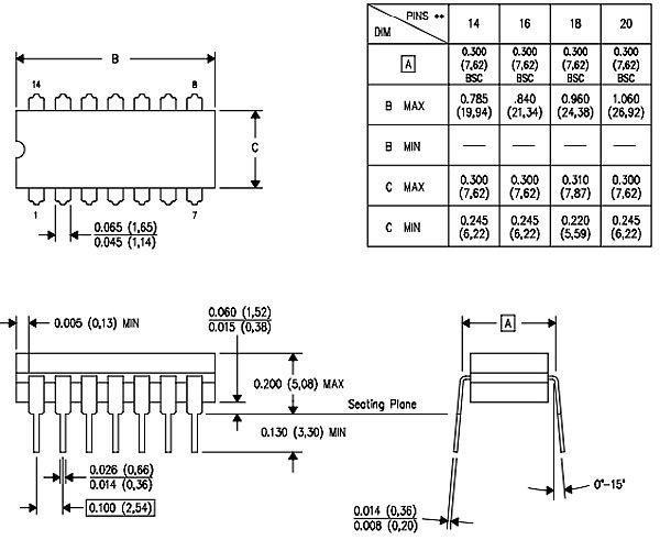
If you want further information on Electrical specification, 2D diagram, you can download the datasheet here:
74LS76 2D Diagram