74LS86 is a quadruple XOR gate digital IC. There are three types of gates AND, NOT and NAND gate but with these gates, we can make multiple gates according to the requirement. Some times these three gates don’t fulfill the requirement then-new gates can be designed with the combination of these three (AND, NOT, OR) gates. When we combine these gates then we come up with multiple gates and XOR is one of them. XOR gates are logic gates with the combination of two NOT, two AND & one OR gate. The output state gets LOW only at the same inputs.
Recommended Components
The following parts are used in this article, along with a generic electronics kit that is handy for building and testing the circuit.
| Component | How it’s used | Buy on Amazon |
|---|---|---|
| 74LS86 quad XOR gate | The 74LS86 quad 2-input XOR gate IC this article covers. | Check Price |
| Electronic component assortment kit (1390 pcs) | A handy assortment of resistors, capacitors, LEDs, diodes and transistors for building circuits. | Check Price |
| Digital multimeter (AstroAI) | Measures voltage, current, resistance and checks continuity while you build and debug. | Check Price |
| Breadboard | Solderless base for prototyping the circuit. | Check Price |
| Jumper Wires | Make the connections on the breadboard. | Check Price |
As an Amazon Associate we earn from qualifying purchases. Prices and availability are accurate as of the date/time indicated and are subject to change.
74LS86 Introduction
The XOR gate can be designed with a transistor or with other gates but that will come up with a circuit large in size, to solve this issue we use 74LS86 IC. The IC 7486 comes up with four internal XOR gates. The IC is smaller in size and it comes up with internal speed protection. It also comes in multiple packages that help to solve the requirement of IC in different devices. The output of the IC comes in TTL which makes it compatible to use with other TTL based devices and microcontrollers. The IC has wide use in designing of an adder at the logic level.
74LS85 Pinout Diagram
Pin configuration of XOR gate 74LS86 is shown here. Details of all pins are listed in the table.
| PINS | DETAIL | |
|---|---|---|
| A1 | Pin 1 | The 74LS86 comes up with four XOR gates and Pin 1 will be used as the first input pin. It will use to input the data to first XOR gate within the IC |
| B2 | Pin 2 | Pin 2 will use as the second input pin. It will also use to input the data to the first XOR gate. |
| Y1 | Pin 3 | Pin 3 is an output pin of the first XOR gate. It will use to receive the output from the first XOR gate. |
| A2 | Pin 4 | Pin 4 will be used as the first input pin for the second XOR gate in the IC. |
| B2 | Pin 5 | Pin 5 will also use as the second input pin for the second XOR gate in the IC. |
| Y2 | Pin 6 | Pin 6 is an output pin of the second XOR gate of the IC. It will give the output of the second XOR gate. |
| GND | Pin 7 | Pin 7 will be used as the ground pin. It will use to make the common ground with power supply and other devices. |
| Y3 | Pin 8 | Pin 8 is an output pin used to receive the output from the third XOR gate. |
| A3 | Pin 9 | Pin 9 is an output pin used to send the first input to the third XOR gate in the IC. |
| B3 | Pin 10 | Pin 10 is also an output pin used to send the second input to the third XOR gate in the IC. |
| Y4 | Pin 11 | Pin 11 is an output pin. It is used to receive the output from the fourth XOR gate. |
| A4 | Pin 12 | Pin 12 is an input pin used to send the first input to the fourth XOR gate of the IC. |
| B4 | Pin 13 | Pin 13 is also an output pin used to send the second input to the fourth XOR gate of IC. |
| VCC | Pin 14 | VCC is a power pin used to power up the IC to make it functional. |
How and Where to use 74LS86?
The 74LS86 follows the simple logic of the main basic three gates. The 7486 consists of a logical circuit using two AND, two NOT and one OR gate. The NOT gate will be used at input pins and at the same time the input will be given to the AND gates without inverting. Then the output from both AND gates will be given to the OR gate and the final output will be received through the OR gate. Here’s the following circuit.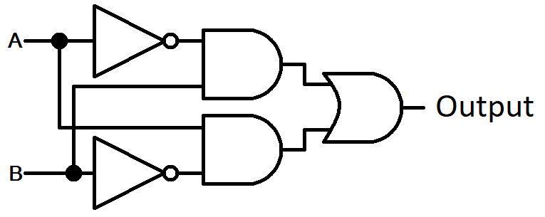
The OR gate only gives the output LOW when both inputs are LOW, here NOT and AND gates are filtering the Both HIGH states to flow towards the OR gates. This simple filtering method makes the XOR gate circuit. The XOR gate can be made up with other combinations too, but every XOR gate will give the specific output on different inputs. The input put and outputs can be represented by a truth table.
Truth Table 7486
| TRUTH TABLE | ||
|---|---|---|
| INPUTS | OUTPUTS | |
| A | B | |
| 0 | 0 | 0 |
| 0 | 1 | 1 |
| 1 | 0 | 1 |
| 1 | 1 | 0 |
Example using 74LS86
In the example of 74LS86, we will design a full adder. In full adder, we will use two XOR gates, two AND gates, and one OR gate. A single XOR gate can be used as half adder but in the single adder, we are unable to get the carry.
Single bit Full adder 74LS86
Here we will design a combination where we will be able to design a full adder using 74LS86. In-circuit there will be three inputs. The first two inputs will be used to enter the two input bits and the third pin will be used as the carrying pin. The full adder we are designing here is only for two bits but we can attach multiple full adders to add more than single bit data. Here’s the circuit.

2 Bit Full adder 74LS86
The full adder circuit will give the output by adding the carry and two inputs. The sum will be represented by a binary number and which will be received from the output of the second XOR gate. The carry out will be the remaining value from the sum and it will also be received as binary. In full adder circuit when we need to add multiple binary digitals, we will use the carry out as the carry-in for the other circuit. Here’s the circuit.
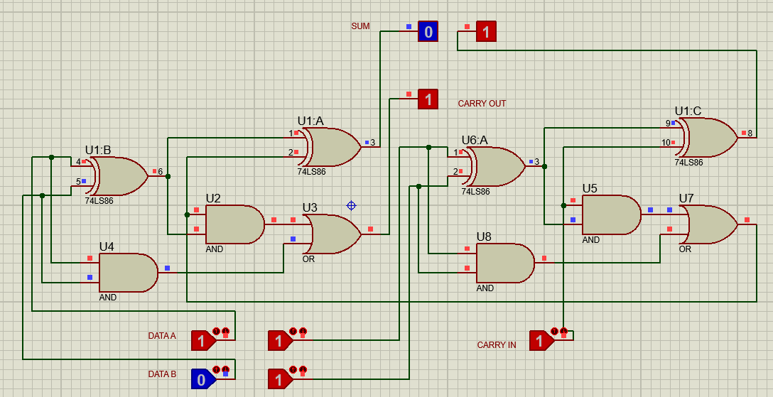
In this circuit, we can view that the carry out of the first adder becomes the carry-in of the second adder. This process will continue further and we can design multiple adders just by following the same circuit. The logic base adder also has premade IC but this logic-based circuit will help us to build an adder in case of emergency or we have a limit where we are unable to use the premade adders. The speed and efficiency of an adder will be the same as compared to the company made adder but its size will be larger.
74LS86 XOR Gate Features
- A single IC provides four XOR gates in different sizes.
- The IC provides output in TTL form, which makes it compatible with other TTL devices and microcontrollers.
- The IC comes in multiple packages, SOIC, PDIP, and SOC.
- The single power supply uses to power up all four gates.
- IC 74LS86 can be used as a single XOR gate without affecting the others.
- Its cost is much less than a transistor-based XOR gate.
SPECIFICATIONS
- The power supply voltage for IC is 4.75 to 5.25. The Power can max up to 7V.
- The output current for the HIGH state is -0.4mA and for the LOW state is 8.0mA
- IC can work up in temperature range from 0 to 70 degrees.
- The input voltage range for the HIGH state is a minimum of 2.0 and 0.8 for the LOW state.
- The input clamp diode can protect up to 1.5V.
- The IC has Propagation delay time for the HIGH state is 22ns and for the LOW state is 17ns.
74LS86 IC APPLICATIONS
- It is used to make the Adder.
- The IC has multiple uses in Networking.
- Servers also have multiple uses of the XOR gate.
- XOR gate is also used in sequence detection for binary data.