74LS IC series comes up with multiple gates. It provides us with compact design and multiple packages of the same IC. Here we will discuss 74LS02. 74LS02 also know as 7402. IT comes up with 4 internal NOR gate. IC 7402 comes up in multiple packages with 14 pins and 2 inputs 4-NOR gates. NOR gate is designed with advanced technology based on silicon. IC 74LS02 internal structure based on CMOS technology. In IC all gates come up with buffered output and it has the ability to provide noise immunity to drive LS-TTL Loads.
Introduction to 74LS02
The IC is functional with all other 74LS logic family and it can be operating with any microcontroller or IC due to its low output compatibility. The interface with other devices doesn’t require any encoder or decoder. Most of the devices come up with 74LS02 due to its cheapness and fast speed. It is possible to design the other AND, OR and NOT gate with 74LS02. This IC also comes up with internal protection from discharge using clamp diodes, which keep it protected from any internal voltage leakage activity.
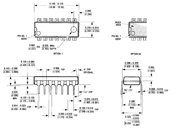
74LS02 pin diagram
This figure shows the pinout of 74LS02 NOR gate IC.

PIN CONFIGURATION Quad 2 input NAND Gate
| PINS | DESCRIPTION | |
|---|---|---|
| 1Y | Pin 1 | Pin 1 is representing the first pin of IC and first OUTPUT of IC. |
| 1A | Pin 2 | Here Pin 2 is representing the first pin of IC and the second pin of First NOR gate. Its state will affect the output of first NOR gate. |
| 1B | Pin 3 | Pin 3 will be the second input of the first NOR gate. |
| 2Y | Pin 4 | Pin 4 will be used as the output of second NOR gate. |
| 2A | Pin 5 | Pin 5 is an input pin. It is used as the first input of the second NOR gate in the IC. |
| 2B | Pin 6 | Pin 6 is the second input Pin of the Second NOR gate in IC. |
| GND | Pin 7 | Pin 7 will be used as the common ground by all the devices and power supply used with the IC to make the ground common. |
| 3A | Pin 8 | Pin 8 will be used as the First input pin of the third NOR gate in IC 74LS02. |
| 3B | Pin 9 | Pin 9 will be the second input pin of the third NOR gate in IC. |
| 3Y | Pin 10 | Pin 10 will be used as the output pin for the 3rd NOR gate. |
| 4A | Pin 11 | Pin 11 will be used as the first input pin of the last and fourth NOR gate of the IC. |
| 4B | Pin 12 | Pin 12 will be used as the second input pin of the fourth NOR gate in the IC. |
| 4Y | Pin 13 | Pin 13 will be used as the output pin for the final NOR gate of the IC. |
| Vcc | Pin 14 | Pin 14 will be used as a power pin to make the IC functional. |
74LS02 FEATURES
- It can be used to design other gates
- IC 74LS02 comes up in multiple packages, SOIC, SOP and PDIP.
- The single IC has four gates that operate on a single power supply pin.
- IC outputs always come in TTL. It is dues to its internal structure based on CMOS.
- It has internal protection from discharging.
- It has a low power consumption
NOR Gate Working
NOR gate use in multiple functions but to understand it working we have to understand its structure. The NOR gate comes up with the combination of OR and Not gate. The combinations of both gates use five transistors 4 resistors and two diodes. The diodes are used to control the one side current flow and transistors and resistors are used as switching. The first two transistors are attached to further transistors each, which gives the output to another transistor.![]()
That makes a total of three transistors for a single input. First, two-transistor do not have any effect on the other until they attach to the third transistor. Whenever the first two-transistor will be used as input and they get a HIGH state then they HIGH state will be given to the third transistor. The transistor will work as an inverter or not gate. The HIGH input will allow the third transistor to give the LOW output and LOW input on the third transistor will give the HIGH output. This whole combination will make the circuit of the NOR gate. The circuit will follow the following formula: (A+B)’ = OUTPUT.
NOR Gate Truth Table
The IC 74LS02 will need only two power to get in the working state. Just apply power then connect it with any TTL device start using it. Every single gate will follow the following truth table.
| INPUT | OUTPUT | |
|---|---|---|
| A | B | |
| 0 | 0 | 1 |
| 0 | 1 | 0 |
| 1 | 0 | 0 |
| 1 | 1 | 0 |
74LS04 CONVERSION to other GATES
NOR gate can be used to convert Into other gates. First, we will convert the nor gate to NOT gate. The NOT gate can be made from the NOR gate just by combining its inputs. Then the NOR gate can be used as NOT gate. To convert the NOR to OR gate we will just have to attach the NOT gate at the end of NOT gate, with that method NOR gate will start acting as OR gate. To Convert the NOR to AND gate just attach two NOT gate made by using NOT gate at the input. Then the NOR gate will start giving the output as AND gate and just by attaching the NOT gate at the end of AND gate it can be used as NAND gate. Here is the symbolic method to convert the NOR gate to the NAND gate.

How to use 74LS04
Here we will use the IC 74LS02 in Proteus to understand the NOR gate output by using logic states. We will convert the one gate as NOT gate and other Two as NAND gate. The give the input and check the output according to the given instructions. Now we will apply the input on NOT gate made by NOR gate and see the output.

You may notice that the input value is inverted and OUTPUT is one. Now we will do the same with the other four gates. Just apply the input 1 and 0. The output will be 0 in case of AND gate otherwise it will be 1 in OR gate.
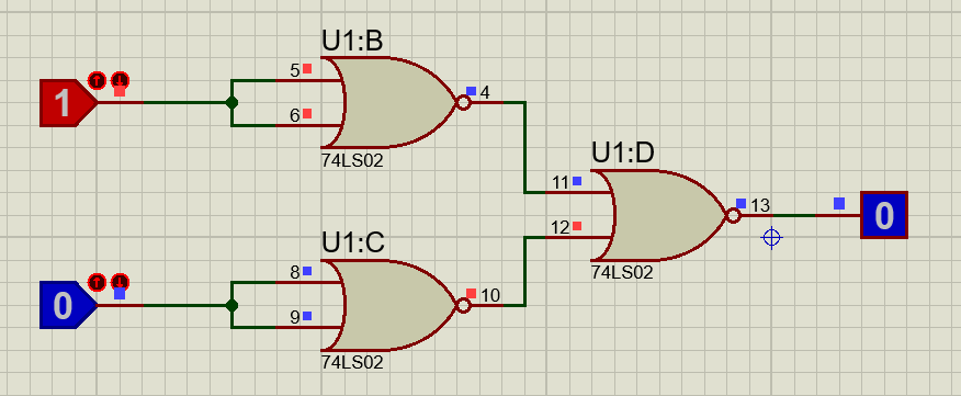
Here you may notice that OR gate is fully easy to work will like other gates. In proteus, the symbols are different for some device for better understanding but their functionality is the same. Whenever we need to work with NOR gate IC, we will just use it like other IC. The Size of IC may be small in real but their speed of work will always be better more than its size.
74LS04 IC APPLICATIONS
- NOR gate can be used as a general use of NOR logic.
- In Digital Electronics, Server and many ALUs also come with NOR gate.
- NOR gate has wide use in Memory units.
- Networking needs NOR gates for some operations.
SPECIFICATIONS
- The operating voltage for the IC I +4.75 to +5.25. The Supply could be extended to 7V.
- The maximum current can draw from the output of the gate is 8mA.
- The maximum ESD protection range for IC is 3.5KV.
- The typical rise and fall time for IC is about 15ns.
- The IC operating temperature is from 0 to 70 degree and its storage temperature range is -65 to 150 degrees.
RELIABILITY
- The IC comes up four internal NOR gates which cost less than making a single NOR gate.
- The single NOR gate can the gate’s output at the same time, instead of using them all.
- The IC can be used to design other gates. A single NOT, AND & OR gate can be designed by using the four gates.
- The chip operates at high speed. The chip is designed by Schottky transistors which minimize the switching delays.
- The IC gives output in TTL states, which makes it workable with other systems.
2D Diagram 74LS02
All dimensions are given inches.