ATtiny85 microcontroller is one of the small and high-performance AVR microcontroller, which is based on RISC CPU. It is one of the 8-pin microcontrollers that comes in two packages, used to control and interfacing between different devices and sensors. It comes with 10-bit ADC and MSSP. ATtiny85 is one of the low power consumptions and a small-sized microcontroller with 8Kb EEROM and 512 bytes RAM which is enough to store the instruction code. The microcontroller also has some safety features like watchdog timer and it has a vast use in automation and other embedded systems, which makes it still reliable till in the modern era.
PIN CONFIGURATION ATtiny85 Microcontroller
Pinout diagram and further explanation of pin configuration for this small Avr microcontroller are listed in this section. All these details are according to its datasheet.
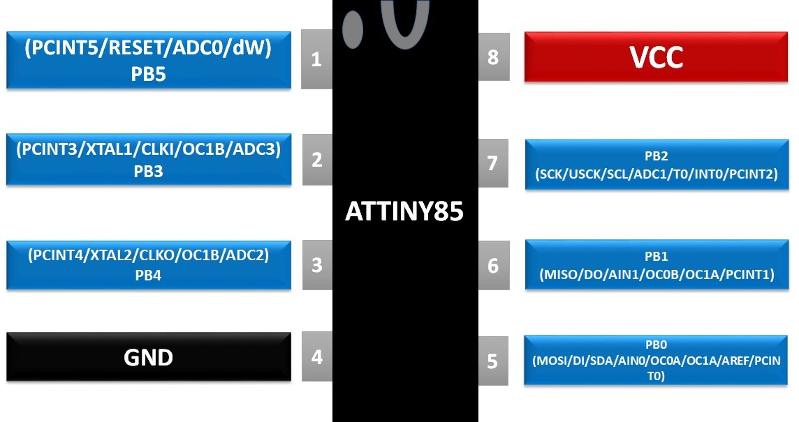
Now, we will discuss the pin diagram details one by one as mentioned in the datasheet.
POWER INPUT: ATtine85 has only two power pins due to its limited number of pins. One of the power pins will be for power input and second will be used for common ground. The power-on microcontroller should not be increased than its designed maximum voltages:
- VCC – Pin8
- GND – Pin4
OSCILLATOR/CLOCK: It comes with an 8MHz internal clock and the value of the clock can be variate from 0-8Mhz but ATtiny85 has the ability to expand the oscillator up to 20MHz. To increase the oscillator value, it should be connected to the oscillator pins of the microcontroller, which are:
- XTAL1/CLKI – GPIO2
- XTAL2/CLKO – GPIO3
DIGITAL INPUT/OUTPUT: In this microcontroller every pin except power pin. ALL input/output pins are connected to bidirectional Input/output register through internal pull-up registers. Any pin can be used for input or output purpose but first, it should be described in a program which function it should follow. All those input/output pins are:
- PB0 – GPIO5
- PB1 – GPIO6
- PB2 – GPIO7
- PB3 – GPIO2
- PB4 – GPIO3
- PB5 – GPIO1
INTERRUPT: To get the attention of the microcontroller by ignoring all the other instructions an external interrupt pins are used, which can be controlled by any sensor output or manual button. ATtiny85 microcontroller has one interrupt pins:
- INT0 – GPIO7
SPI: Sensor uses multiple kinds of serial communication and SPI is one of them. ATtiny85 gives the ability to operate with other devices through SPI protocol, it is also helpful in case of multiple peripheral but here it is only used by a single device in case of SPI data communication and to program the microcontroller. The SPI pins in this microcontroller are:
- MOSI – GPIO5
- MISO – GPIO6
- SCK – GPIO7
- dW (debug wire) – GPIO1
MOSI pins are used to send the data from controller, MISO is used to receive the data and SCK is for clock pulse. Debug wire will only use in case of programming.
I2C: ATtiny85 also have I2C communication protocol ability. I2data is being sent and received by a single line and another line is used to send the clock pulse to keep the data sync according to the time. ATtiny85 also has I2C pins which are:
- SDA (Data) – GPIO5
- SCL (Clock) – GPIO7
TIMER: In this microcontroller, there are two timers, both of these timers can be used to count the pulses. The Timer0 and Timer1 both can be work according to the internal clock but Timer0 can be operated with the external clock pulse. Both of these timers are 8-bit. Timer/Counter pins in this PIC are:
- T0 (Timer0) – GPIO7
TIMER/COUNTER/COMPARE: In ATiny85 there are some special pins which can be used to drive the external power safely by a combination internal PWM signal input. These pins are able to operate according to specific time which is called Dead Time Generator. The timer starts counting and keeps comparing its value until it reaches zero. In ATtiny85 two dead time generators are used by counting through Timer0 and Timer1 and output signal comes in both inverted and non-inverted form, in other words, we say in non-overlapping form. The List of these pins are:
- OC1B – GPIO
- OC1B’ – GPIO
- OC0B – GPIO
- OC0A – GPIO
- OC1A – GPIO
- OC1A’ – GPIO
ANALOG COMPARATOR: Comparison of an analog signal can also be done in ATtiny85. It has an internal Analog comparator which can be used to compare the same analog signal (inverting and non-inverting). The output of their comparison store within the register and can be used further. The analog comparator input pin of ATtiny85 are:
- AIN0 – GPIO5
- AIN1 – GPIO6
ANALOG TO DIGITAL CONVERTER: ATtiny85 has 4 analog input channels. The analog input is converted into 10-bit digital output. ATtiny85 convert the analog data at the 65-260us speed which is enough to keep the system update at every second. Analog input voltage level is decided according to the power supply voltage, which can be some time cause error for external devices. To remove this issue an analog reference pin is used, which helps the system to understand the voltage maximum and minimum level according to the given voltage reference. The reference voltage and analog input signal voltage should not be exceeded from the actual voltage handling power of the controller. Analog pin of ATtiny85 are:
- ADC0 – GPIO1
- ADC1 – GPIO7
- ADC2 – GPIO3
- ADC3 – GPIO2
- Vref – GPIO5
RESET: Microcontroller also comes with an external and internal reset. It can be reset from the program on a specific condition or it can be controlled from an external pin.
BLOCK DIAGRAM
The block diagram of the microcontroller ATtiny85 is:

APPLICATIONS
- ATtiny85 used in development boards and hobbies projects.
- In the industrial control system, the PIC is used due to its multiple functionalities due to a specific operation on special conditions.
- PIC is also used for analog manipulation and its measurement.
- In small commercial devices, the PIC ATtiny85 is used.
ATtiny85 microcontroller PERIPHERALS
There are multiple modules within the controller but all of them are independent on registers to operate. For details and further information on their registers for programming, you can go through the datasheet.
BROWN OUT RESET: Brownout reset is used within the IC, which protect it in low voltage situation. Whenever the voltage will lower down from threshold then it will reset the IC and multiple voltage ranges are also used to protect the IC.
WATCHDOG TIMER: It is one of the best resetters in most of the microcontroller. To activate it only instruction will be given at the start of the program. It will not affect anything of the controller unless the controller stops operating and then watchdog timer will reset the ATtiny85 and will start it again.
DEBUG WIRE: In SPI pins you may notice that we talked about SPI programming method to the PIC but to program any controller through the SPI protocol a debug pin will be used which will cut the program instructions from the CPU and then it will program the non-volatile memory. The use of a debug pin will be only in case of SPI pins are present on the controller otherwise it won’t have any specific use.
DEAD TIME GENERATOR: It is the output pairs of PWM within the ATtiny85 which allows the controller to control the external control switches safely. It operates by using a PWM pulse and a zero check is used with the Dead Time Generator to check the counter has been finished. The Dead Timer Generator helps the output two be non-overlapping.
SELF PROGRAMMING: ATtiny85 comes with a self-programming feature which can be used to set the bootloader of the controller. This self-programming method I helpful in case of a memory issue for a commercial product. It can also be used to receive specific data during the bootloader. To use the self-programming feature the controller will need to enable this feature first otherwise it will not work.
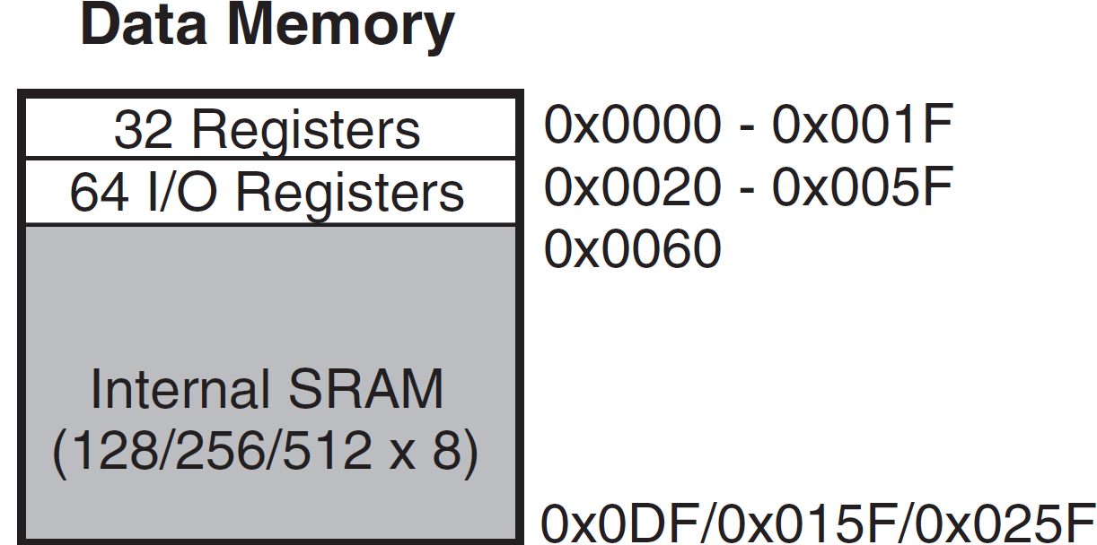
MEMORY MAP
The total memory map of ATtiny85 is given below:
ATtiny85 Features
| Name | Features |
|---|---|
| CPU Architecture | 8-bit RISC Architecture |
| CPU Frequency | , 0 – 20 MHz |
| Operating Voltage Range | 4.5 – 5.5V |
| GPIO PORTS | 6 I/O Pins |
| Interrupts | One External interrupt on INT0 – GPIO7 |
| Timers |
|
| PWM | 2 PWM channels |
| UART | Not Available |
| I2C | One I2C channel |
| SPI | One SPI communication channel with pins: MOSI – GPIO5, MISO – GPIO6, SCK – GPIO7 |
| LAN | No Available |
| CAN | No Available |
| ADC | 4-channel, 10-bit ADC |
| DAC | No Available |
| Enhanced USART Module | 1 Channel |
| SRAM | 256 bytes |
| FLASH ( Program Memory) | 8K bytes |
| EEPROM | 512 bytes |
| Comparator | one analog comparator with input pins as AIN0 – GPIO5 AIN1 – GPIO6 |
ATtiny85 Microcontroller Programming
To program Atmel microcontrollers, we always need a compiler. These are the popular compilers used for programming in c language or assembly language.
- Atmel Studio ( Getting started guide on Avr studio)
- Mikro C for AVR
- AVR – GCC
- AVR – toolchain for Windows and Linux
GPIO Programming Example
Now let’s see an example of using GPIO ports. In this programming example, we will set pin 0 and pin 1 of port B as digital high. Pin 2 and Pin 3 of Port B digital low. We also declare GPIO4 and GPIO5 as digital input pins.
PORTB = (1<<PB4)|(1<<PB1)|(1<<PB0);
DDRB = (1<<DDB3)|(1<<DDB2)|(1<<DDB1)|(1<<DDB0);
LED Blinking Program Example
We see an example of an LED blinking with a push button.
#include <avr/io.h>
int main(void)
{

   // Set the port b pin 4 as a digital output pin
   // Connect LED with this pin

  DDRB |= (1 << PB4);
   // Set pin 5 of port b as a digital input pin
   // Connect switch with this pin

   DDRB &= ~(1 << PB5);
   //Enable pull-up resistor of PB5

    PORTB |= (1 << PB5);

    while(1)

    {

   // Check if switch is open, LED remains off
        if (PINB & (1 << PB5))
       {

            PORTB &= ~(1 << PB4);
      }

   // Check if switch is closed, turn on the LED
        else {

            PORTB |= (1 << PB4);

        }

    }
This code simply turn on an LED connected with PB5 according to state of switch that we connect with PB4.
Good post
Very helpfull,thank you