In this tutorial, we will discuss the workings of a binary-weighted resistor DAC. It consists of an inverting amplifier op-amp and a string of weighted resistors to distinguish each bit starting from the LSB to the MSB position. Each resistor represents a digital bit to be converted into analog form.
The maximum amount of information in the real world is in analog form. For example, data from sensors, audio applications, and multimedia are all in analog form. Therefore, we use DAC and ADC to convert data from one form to another, and we digitize these signals for fast computing, which saves us time and allows us to process complex data in a few microseconds. But the real world is unable to understand these combinations of binary bits, which is why we need to convert them back into analog information with the help of a DAC.
What is a DAC?
A DAC is an electronic circuit that takes in digital data as input and transforms it into an analog output signal. It is actually the output voltage proportional to the binary code given at the DAC input and then used to drive various circuits. They have vast applications, but let us take a simple example of an audio system to showcase their importance.
The DAC in the audio system takes in the audio binary data. It processes and converts all the 0s and 1s to a continuous analog signal, which is then transmitted to an amplifier. Thus, the sound we hear from the speaker is the amplified analog signal.

There are different types of DACs implemented with a special technique to generate analog output, but this post will overview the binary weighted resistor DAC.
Binary Weighted Resistor DAC
It is the type of DAC that transforms a particular binary code into an equivalent analog signal. Thus, if the binary code given at the input terminal is altered continuously, the output will change as well. So, this type consists of weighted resistors whose values are kept as multiples of two and an inverted summing operational amplifier, which results in an output signal with a 180-degree phase shift. The reference voltage is either generated internally or provided to the DAC converter to determine the maximum output voltage of the converter.
Before discussing the transfer function of the binary-weighted resistor DAC, we should be familiar with resolution and full-scale output voltage.
DAC Resolution
The resolution of an ADC is given by the number of bits. It depicts the number of output levels a DAC can generate. The general formula for resolution is:
Resolution = 2^N
Where N represents the number of bits. For a 4-bit DAC, the resolution will be 16.
Step Size
It is the smallest change that a DAC can produce in the output, or we can say that it is a difference between two consecutive voltage levels of the DAC. It is determined by dividing the reference voltage by 2, with power equivalent to the number of bits.
Step size = Vref / 2^N
The reference voltage is also multiplied by a factor, i.e., the internal gain of the ADC, which depends on the design of the DAC.
The resolution and step size are inversely related to each other. Increasing the resolution decreases the step size between the output levels, which leads to smooth and precise analog output.
Full-scale Output Voltage
The maximum voltage that we can attain from a DAC has a name, which is full-scale output voltage. The FSO voltage depends entirely on the number of bits and the reference voltage given to the digital-to-analog converter. We can obtain this via the following formula:
FSO = (2 * N – 1) x Vref / 2 * N
Binary Weighted Resistor DAC Working
The configuration uses a summing amplifier whose output voltage is proportional to the sum of the voltages applied at the input.
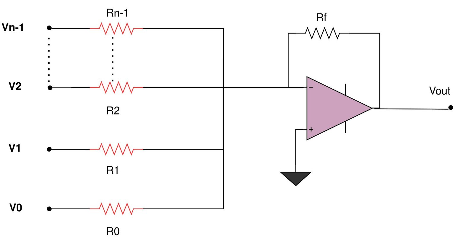
Vout = – {(Rf / R0) V0 + (Rf / R1) V1 + (Rf / R2) V2 +… + (Rf / Rn – 1) Vn – 1}
Circuit Diagram
If resistors with precise values connect with each of the input voltages to scale the gain, it starts working as a DAC. All the input voltages connect to the same reference voltage, so the formula becomes:
Vout = – {(Rf /R0) Vref + (Rf /R1) Vref + (Rf /R2) Vref +… + (Rf/Rn-1) Vref}
Vout = – Vref {(Rf /R0) + (Rf /R1) + (Rf /R2) +… + (Rf/Rn-1) }
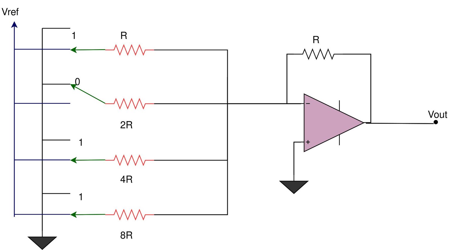
In the circuitry, we apply the binary input through digital switches that alter the reference voltage and ground. If we want the input bit to be 1, the switch should connect to Vref, and for digital input 0, it should connect to ground. In the equation given below, B0 is the least significant bit, and Bn-1 is the most significant bit.
Vout = – Vref { B0 (Rf /R0) + B1 (Rf /R1)+ B2 (Rf /R2) +… + Bn-1 (Rf/Rn-1) }
For compactness, Rf = R, whereas the weighted resistors, i.e., R0, R1, R2,…, Rn-1, are scaled with the scaling factor 2(N-1)-n to give the output gain according to the weight of each bit.
Rn = 2(N-1)-n R
where N represents the number of bits and n is the bit position. So, the generalized output of the binary weighted resistor DAC is given out as:
Vout = – Vref { B0 (R/2(N-1) R) + B1 (R /2(N-2) R) + B2 (R /2(N-3) R) +… + BN-2 (R /21 R) +BN-1 (R /20 R) }
Vout = – Vref { B0 (1/2(N-1)) + B1 (1 /2(N-2)) + B2 (1/2(N-3)) +… + BN-2 (1 /2(1)) +BN-1 (1 /2(0)) }
4-bit Binary DAC Equation
For a 4-bit binary DAC, the output voltage equation is:
Vout = – Vref { B0 (1/23) + B1 (1 /22) + B2 (1/21) + B3 (1/20) }
Vout = – Vref { B0 (1/8) + B1 (1 /4) + B2 (1/2) + B3 }

Binary Weighted Resistor DAC Example
Let us take the example of a 4-bit binary code. Assuming Vref = 5 V and code = 1011, the weighted output voltage is:

Vout = – 5 { 1 (1/23) + 1 (1/22) + 0 (1/21) + 1 (1/20) }
Vout= – 5 { (1/8) + (1/4) + 0 + 1 }
Vout= – 6.875 V
Remember that B0 is the LSB and B3 is the MSB.
As this is a 4-bit DAC, we can have 16 different combinations of binary code, each producing a specific output voltage limited to the reference voltage. The table below provides the output voltage corresponding to every possible 4-bit code.
| Binary Inputs | Vout | |||
|---|---|---|---|---|
| B3 | B2 | B1 | B0 | Volts |
| 0 | 0 | 0 | 0 | -0 |
| 0 | 0 | 0 | 1 | -0.625 |
| 0 | 0 | 1 | 0 | -1.25 |
| 0 | 0 | 1 | 1 | -1.875 |
| 0 | 1 | 0 | 0 | -2.50 |
| 0 | 1 | 0 | 1 | -3.125 |
| 0 | 1 | 1 | 0 | -3.75 |
| 0 | 1 | 1 | 1 | -4.375 |
| 1 | 0 | 0 | 0 | -5.00 |
| 1 | 0 | 0 | 1 | -5.625 |
| 1 | 0 | 1 | 0 | -6.25 |
| 1 | 0 | 1 | 1 | -6.875 |
| 1 | 1 | 0 | 0 | -7.50 |
| 1 | 1 | 0 | 1 | -8.125 |
| 1 | 1 | 1 | 0 | -8.750 |
| 1 | 1 | 1 | 1 | -9.375 |
The table shows the LSB, or step size, with a measurement of -0.625 volts, while the MSB, or full-scale voltage, turns out to be -9.375 volts.
Drawbacks
- The binary weighted DAC has quite a large gap between LSB and MSB resistors values and requires a very precise value of resistors.
- Hence, it becomes impractical for higher-order DACs and is suitable for lower-resolution DACs.
- The stability of the device is resistor-dependent. It is difficult to maintain an accurate resistance ratio with temperature variations.
Advantages
- It has a simple assembly.
- It has a fast conversion speed.
- Simple conversion circuit
You may also like to read:
- R-2R DAC and DAC IC’s
- DAC7715 Digital to Analog Converter
- DAC STM32F4 Discovery Board
- PT8211 16-Bit DAC
- DAC0808 8-bit Digital to Analog Converter
- How to use DAC Module of Pic Microcontroller
- DAC0832 8-BIT DIGITAL TO ANALOG CONVERTER IC
This concludes today’s article. If you face any issues or difficulties, let us know in the comment section below.
Resolution=2^N, not Resolution=2N
Thanks for pointing out a typo. We have fixed it.