Recommended Components
The following parts are used in this article, along with a generic electronics kit that is handy for building and testing the circuit.
| Component | How it’s used | Buy on Amazon |
|---|---|---|
| CA3130 BiMOS op-amp | The CA3130 MOSFET-input BiMOS op-amp this article covers. | Check Price |
| Electronic component assortment kit (1390 pcs) | A handy assortment of resistors, capacitors, LEDs, diodes and transistors for building circuits. | Check Price |
| Digital multimeter (AstroAI) | Measures voltage, current, resistance and checks continuity while you build and debug. | Check Price |
| Breadboard | Solderless base for prototyping the circuit. | Check Price |
| Jumper Wires | Make the connections on the breadboard. | Check Price |
As an Amazon Associate we earn from qualifying purchases. Prices and availability are accurate as of the date/time indicated and are subject to change.
CA3130 Pin Configuration Diagram
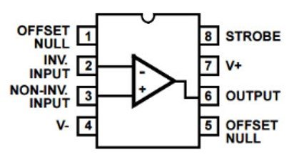
Pin Description
Pin# 01, 05: OFFSET NULL
When the input pins of the op-amp are connected with each other, the voltage at the output should be zero. But no operational amplifier is perfect. Therefore, there is a small offset when the two inputs are shorted together. The offset null pin is used to null these offsets by applying the voltage between the two input terminals of an operational amplifier to null the output voltage.Pin#2: INV. INPUT
It is the inverting/negative input terminal of the operational amplifier integrated inside the IC.Pin#3: NON-INV. INPUT
It is the non-inverting/positive input terminal of the operational amplifier integrated inside the IC.Pin#4: V-
It is the connection for ground or negative power supply.Pin#6: OUTPUT
It gives an amplified output signal.Pin#7: V+
It is connected to a positive power supply.Pin#8: STROBE
This pin is used to shut down the output stage. When it is connected to the negative supply, the output value at pin 6 will rise to the potential of the positive supply. It can also be used for phase compensation in comparators.CA3130 Mosfet Op-mp pinout Features
- Operational amplifier IC having MOSFET at the input stage.
- It can perform both single supply and double supply operations, but it is ideal for single-supply operations. The ranges of voltage are:
- Single supply voltage range: 5V to 16V
- Dual supply Voltage range: ±2.5V to ±8V
- Supply current is 10mA.
- Maximum output voltage is 13.3V.
- It has a very low input current of 1mA.
- Maximum source and sink currents are 22mA and 20mA.
- Common-mode input voltage range includes the negative supply rail and the input terminals of this IC can be swung 0.5V below that negative rail.
- The common-mode Rejection Ratio (CMRR) is 80dB.
Where to use it?
It is normally used for amplification purposes. It can be used as a comparator, voltage followers and voltage regulators by adding external components. You can use this IC in applications requiring low input current, high input impedance, and high bandwidth.How to use a CA3130 IC?
It can perform single and dual supply operations. The circuits are given for both operations. The only difference between them is in single-supply operation, the fourth pin is grounded.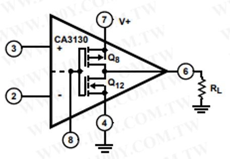
 Pin 8 can strobe the output stage into quiescence. It can be also used for phase compensation to drive CMOS digital circuits in Comparator applications. Offset nulling can be achieved by connecting a 100,000Ω potentiometer across pins 1 and 5. The slider arm of a potentiometer is connected to pin 4. A fine value can be obtained by sliding the sliding arm. A small capacitor is connected between pins 1 and 8 for achieving effect compensation. A capacitor of value 47pF is suitable for providing enough compensation for stable unity-gain.
Full Wave Rectifier Example CA3130
This circuit shows an example of full-wave rectification using Mosfet built-in operational amplifier IC. This circuit uses only a single power supply.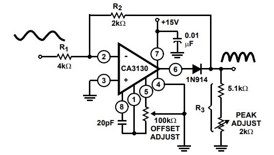
Pulse Generator Circuit using CA3130
This circuit generates pulses of different frequency and pulse period. You can select frequency and pulse period with the help of a switch S1.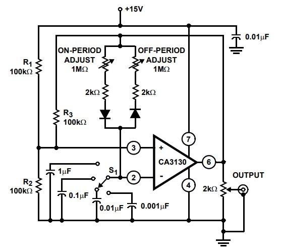
Applications
- Due to their high input resistances, they are suitable for designing voltage followers and multivibrators.
- Function generators use it as an integrator and in threshold detector functions.
- It can be used to perform frequency to voltage conversions and temperature to frequency conversions by using external components (including resistors, capacitors, etc) along with this IC.
- It is used for designing of Digital to Analogue converters and oscillators,
2D Diagram
