CD4015 IC is a static 4-stage data shifting IC consisting of two independent Shift Registers. These two shift registers provide serial input / parallel output registers. in other words, shift registers convert serial data into parallel data. The date that this CD4015 can convert is 4 bit. All inputs are protected by diodes and series resistors to protect them against static discharges. All register stages are composed of D type, master-slave flip flops with independent RESET and CLOCK inputs. It is available in 16-pin packages which include PDIP, GDIP, PDSO.
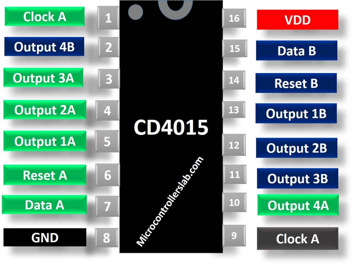
CD4015 Pinout diagram
As you can see from the pinout diagram, the CD4015 shift register IC consists of 16 pins. Blue color shows pins of register B and Green color depicts pins of shift register A.
Pin Configuration Description
The CD4015 IC has a total of 16 pins. Each pin, its number, and description are mentioned in the table below.
| Pin Number | Pin Name | Pin Description |
|---|---|---|
| 1 | Clock B | Clock pulse signal for shift register B |
| 2, 11, 12, 13 | 1B, 2B, 3B, 4B | Output pins for shift register B |
| 3, 4, 5, 10 | 1A, 2A, 3A, 4A | Output pins for shift register A |
| 6 | RESET A | Responsible for resetting all the outputs of a shift register A |
| 7 | DATA A | Input data pin for shift register A |
| 8 | Vss | Negative power supply or ground of the circuit |
| 14 | RESET B | Responsible for resetting all the outputs of a shift register B |
| 15 | DATA B | Input data pin for shift register B |
| 16 | Vcc | Power supply voltage |
Other alternative and Equivalent shift Registers: 74HC595, CD4035,, CD4014, CD4022
CD4015 Static Shift Register Features
- Dual 4-bit IC having serial Inputs and a parallel output Shift register composed of 8 master-slave flip flops.
- Fully static operation with a clock frequency of 8.5Mhz at 15V
- Operating voltage range is 3V to 18V with medium speed operation
- Consumes low power of 80uA
- TTL compatible
- Maximum Clock Frequency is 12Mhz at 10V
Alternative options
Where to use CD4015 IC
It is commonly used in high voltage applications as it has a wide operating voltage range. It can also be used as an I/O expander to control multiple outputs. It can be used in applications that require controlling multiple outputs in a parallel mode as it has 8 parallel outputs. Due to its large number of outputs, you can expand the I/O capability using this IC. You can use it in LED chasers and LED drivers.
How to use a CD4015 IC

The IC consists of two 4 stage shift registers. Each register has its own 4 bits input, a RESET pin, and a Clock. The clock signal is provided through a PWM signal generated through a 555 timer or any other digital IC. This is a functional block diagram of IC:

The pins 1 and 9 are clock inputs that provide a constant signal. It has only 1 data input pin. The data value present at this input is transferred into the first register stage on the positive edge of a clock. At each positive transition of a clock, this data is shifted over one stage. The rest pin is responsible for resetting all the output values. When this pin is HIGH, it resets output pins. The reset pin is normally connected to the ground of the circuit. The truth table showing the state of the register after the positive transition of clocks is shown in the table below.

Example Circuits

- In this example circuit, we connect serial data 0001 to serial input pin15 (Pin D) and a clock signal to pin1.
- We can use the Probestate of proteus to see the output from pins Q0-Q3.
- As soon as we apply a clock signal to CD4015, data will start to shift on the output pin.
- Because input data is 0001, 1 will appear on Q0 on the fourth edge of the positive clock cycle.
CD4015 Proteus Simulation
- For simulation purposes, we are using logic states and logic probes of proteus. We will provide clock signal and serial data input through these logic states.
- For simulation purposes, We will use the toggle switch to provide a positive edge. Because, switching from zero to one, will provide a positive edge, to shift register.
- We can use the Probe state of proteus to see the output of Q0 to Q3.
- Now let’s see proteus simulation working,
- First makes serial data input pin logic high, that means, logic one will transfer to each stage on every positive edge of the clock cycle, Because in serial mode, data transfer bit by bit.
- Hence, on the first positive edge, pin Q0 will become one, on the second positive edge of the clock, pin Q1 will become high, and so on.
- After that, apply the clock signal and see the output of the shift register. As you can see, as soon as we apply a clock signal to CD4015, data will start to shift on the output pins.
- Now change the serial data input to logic low,
- In the end, apply the clock signal, as you can see, logic zero appears on pin Q0 and other pins sequentially on every positive edge of the clock,
Applications
This IC has numerous applications. Some of them are:
- It can be used in serial to parallel data conversion as it has serial input and parallel data outputs.
- Due to its multiple outputs, it is used in LED matrix projects in which LEDs are interfaced with the outputs.
- It can be used in cascading applications by connecting multiple IC’s of CD4015.
- Cube Projects and High logic level controllers also use this IC
- In communication lines for transmitting and conversion of data.
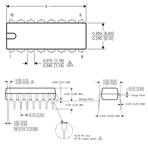
2D Diagram