The CD4049 IC is a CMOS logic-based hex inverter IC consisting of six inverters on a single package. We can use it in high voltage applications as it has a wide range of operating voltage from 3V to 18V. As it is an inverter IC and the function of an inverter is to convert the logic level HIGH to LOW and LOW to HIGH, therefore it is used in logic level conversions. More than 18V can damage the IC but the input voltage signal value can be greater than supply voltage especially in conversion of logic levels.
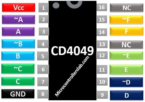
CD4049 Pinout Diagram
This pinout diagram shows that this hex inverter buffer has 6 inverter or NOT gates. Two pins are marked as NC that means no connection.
Pin Configuration Details
This IC has sixteen pins. The description of all these pins are mentioned in the table below
| Pin No. | Pin Name | Description |
|---|---|---|
| 1 | Voltage supply | |
| 3, 5, 7, 9, 11, 14 | A, B, C, D, E, F | Input pins of the inverter |
| 2, 4, 6, 10, 12, 15 | G, H, I, J, K, L | Output pins of the inverter |
| 8 | Ground of the circuit | |
| 13, 16 | NC | Not Connected |
CD4049 Hex Inverter Features
- Inverting IC that can convert High logic level to Low level
- High source and Sink Current as it has the capability of driving 2 TTL Loads at 5V over full temperature range.
- 100% Tested for Quiescent Current at 20 V
- Maximum Input Current of 1 µA at 18 V Over Full Package Temperature Range; 100 nA at 18 V and 25°C
- 5-V, 10-V, and 15-V Parametric Ratings
- It is available in 16 pin packages of PDIP, SOIC, TSSOP, SO.
- Special input protection to protect inputs against static discharges.
Equivalent ICS
Where to use it?
You can use this IC for making simple clock pulse generators and oscillators. CD4049 IC can be used in all those applications whose operation depends on two states 0 or 1 for example in simple LED torch, automatic streetlights, etc. Simple toggling circuits, voltage multiplier circuit, and a square wave oscillator circuit can be designed using this IC. It can also be helpful in inverting the output.
How to use CD4049 Hex inverter?
The operation of this IC is simple as it simply inverts the output.
Truth Table
The truth table of a simple NOT gate is:
| Input | Output |
|---|---|
| 0 | 1 |
| 1 | 0 |
All the NOT gates inside this IC will behave in a similar manner.
Example Circuits
Now, we will see some example circuits using CD4049 Hex inverter IC.
Pulse Generating Circuit
You can design a simple pulse generating circuit by using a resistor, capacitor and the IC CD4049 as shown in the circuit diagram.
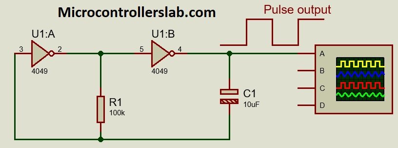
The output frequency is given by the following equation:
F = 1/ 1.39xRxC
Torch circuit using LEDs
Similarly, we can also design a simple torch circuit using CD4049. You can see from the diagram output of gate 1 connects to the input of gate 2 and the output of gate 2 to the input of gate 3. Gate 3 output connects to the LEDs connected in series with 2 other LEDs. Three LEDs are used for bright illumination and they are connected in series in order to save battery life.
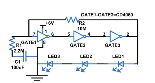
The resistor and capacitors used in the circuit will cause amplification of the signal. When input at pin 7 is LOW, the output at pin 2 will be HIGH and LEDs will glow. The torch will turn OFF when a HIGH signal is applied to the pin 7 input. This IC has many applications. It offers design in many other circuits like those mentioned above.
CD4049 Applications
This IC is normally used in logic level conversions. Some other applications include:
- Designing Square wave oscillators
- Voltage Multiplier circuits
- CMOS to DTL or TTL Converters
- Toggling or ON-OFF circuits
- Current Sink or Source Drivers
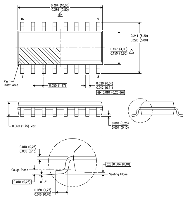
2D Diagram
This two-dimensional diagram of DIP package helps to design a printed circuit board. You can download datasheet of IC for 2D packages of other layouts.