CD4060 IC is a 14-stage counter and counter is a binary ripple carry type. It is a CMOS logic-based binary counter belonging to a CD4000 series of integrated circuits. It consists of a 14-stage ripple carry binary counter along with an internal oscillator. Additionally, we can configure crystal oscillators with RC circuits or external crystal. Moreover, it has a reset circuit that can makes the counter start from all zero’s again. It operates over a power supply range of 3V to 15V. It is available in a variety of 16-pin packages which include PDIP, CDIP, SOIC, TSSOP.
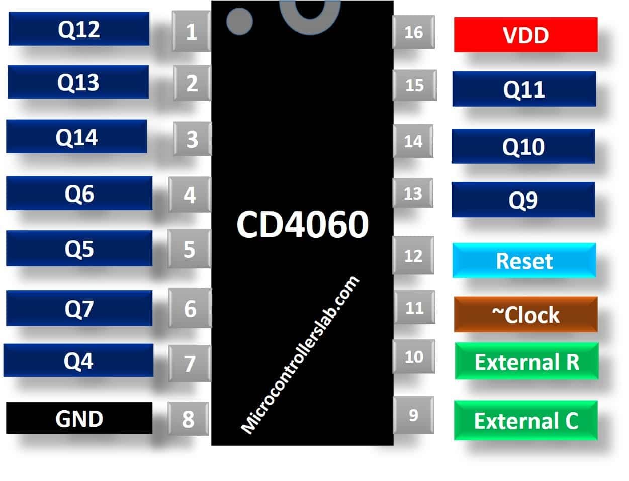
CD4060 Pinout diagram
CD4060 binary counter IC consists of 16 pins. Q4 – Q14 are output pins. These pins offer binary counter output on every positive edge of the clock cycle. Pins that we use to connect the oscillator circuit are Pin 9-10. This simple diagram shows a pin configuration diagram.
Pin Configuration Description
As we mentioned earlier, this IC has 16 pins in total. Each pin, its name, and description are given in the table below.
| Pin Number | Pin Name | Description |
|---|---|---|
| 1, 2, 3, 4, 5, 6, 7, 13, 14, 15 | Q12, Q13, Q14, Q6, Q5, Q7, Q4, Q9, Q8, Q10
| Output pins |
| 8 | Vss
| Ground of the circuit |
| 9 | External connection with capacitor for setting clock frequency
| |
| 10 | External connection with resistor for setting clock frequency or Oscillator pin
| |
| 11 | Clock pulse for setting frequency of clock | |
| 12 | RESET | Resets the value of counter to 0 and disables the oscillator
|
| 16 | Voltage Supply |
CD4060 Binary Counter Features
- Schmitt triggered inputs which allows unlimited rise and fall times
- Fully Static operation with buffered inputs and outputs
- Counting range: 0 to 16383 (In decimal)
- Maximum Clock Frequency is 30MHz at 15V
- Medium speed operation: 8MHz typ. at VDD = 10V
- Pins and function compatible with TTL series
- Reset Propagation Delay: 25ns at 5V
- RC Oscillator Frequency of 690kHz Min. at 15V
Where to use Binary Counter?
CD4060 is an oscillator and counter IC with 10 outputs and can be used in applications that require discrete and accurate variable time delays. On top of that, it can also be used for acquiring high grade and accurate oscillations of frequencies. It is best for use in timing applications. If you want to design a simple but reliable time delay circuit with a few components, then you can use this IC.
CD4060 Working Principle
The CD4060 IC has an in-built oscillator module. As it is a binary counter, therefore on every negative transition of clock pulse, the counter value gets incremented by 1 in binary numbers. The reset input should always be grounded or connected to the negative power supply. If a positive signal (1 or HIGH) is applied to this input, it will reset the counter or oscillations to start from beginning. The effect of reset value and clock pulse is shown in the table below where X is the don’t care condition.
Truth Table
| RESET | Counter Value | |
|---|---|---|
| X | 1 | Reset Counter to 0 value |
| Negative Transition | 0 | Value in counter is advanced by 1 step |
| Positive Transition | 0 | No change |
How to set oscillator Frequency?
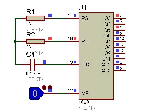
CD4060 has an inbuilt oscillator whose value is determined by the external capacitor connected to pin 11 and resistances connected to its pin 9 and pin 10. Time delay can be changed by varying the value of capacitor or resistor. The value of the resistor at pin 11 should be roughly 10 times that of pin 10 resistor’s value and the free ends of all these components are joined together as shown in the proteus circuit. The formula for finding the oscillation frequency is:
f= 1/ ( 2.5 x R1 x C1)
You can also set the desired frequency by adjusting the values of R1 and C1 in the above equation. In this example, we use R1=1M ohm and C1=0.22uF. Now, let’s put these values into frequency formula:
f = 1 / (2.5*1000000*0.00000022)
f = 1.8 Hertz
Therefore, with these capacitors and resistor values, the clock frequency is 1.8Hz. In the same way, the clock period is 1/f that is 1/1.8 = 0.56 Seconds. But all output pins states will not change according to this time period. However, they will change state in multiple of this oscillator time period. We will explain this in the next section.
To start the oscillator, Turn ON the power supply. The oscillator of the IC would start oscillating. To stop or reset the oscillations, apply logic 1 or a positive supply to the RESET pin.
How to calculate timing of Output pin?
The frequency of each output pin of CD4060 obtained will be double the previous one. If the frequency at pin 3 is 4Hz, then at pin 2 it will be 8Hz and so on. In addition to it, we can calculate the time period of each pin by this formula:
T = 2^n / fosc
In this formula, fosc is the frequency of the oscillator. Also, n is an output pin number. For example, if we want to determine the transition time of pin Q6. Consequently, n will be equal to 6. Now just put these values in above formula.
T= 2^5/1.8= 64/1.8= 35.5 seconds.
Therefore, we will get a logic high output at pin Q6 after 35.5 seconds.
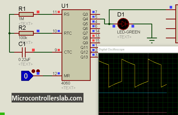
CD4060 Example Circuits
This is an example of an LED blinking circuit using a binary counter. As you can see from the image that this circuit flashes LED after every one second.
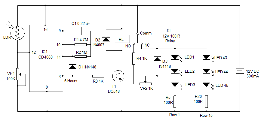
CD4060 Example Controlling street light
This CD4060 Example circuit controls the street light with 6 hours delay. We can a Light-dependent resistor with a reset pin. LDR senses light and provides reset signal to the timer when light falls below a certain level. But as soon as it detects low light, CD4060 timer becomes active. But LED lights turn on after the delay of 6 hours. Because crystal oscillator frequency is selected this way.
CD4060 Applications
CD4060 IC has numerous applications. Some of them are given below:
- Timers
- Time Delay Circuits for creating long time delays
- Frequency divider
- counter circuit
2D Diagram
When we design PCB for electronics projects, we have to keep in mind the dimension of an electronics component. This is a 2D physical dimension diagram for the DIP package.

This is a comprehensive explanation on ic 4060. Thanks
Hi,
Just wanted to say this is a great well presented tutorial on the 4060 14 stage ripple counter. The datasheet should but doesn’t provide details like you have in your youtube presentation and this is a must for anyone who really wants to know more about specific components. There is plenty of circuits for this specific IC on the net with no supporting info and a lot of it is duplicated from other sites it is really good see this keep up the good work.
Hi,
Thanks for your supportive words. We try our best to provide in-depth details on topics under discussion with easy to follow examples.
the reset pin per spec sheet does not have a schmidt trigger . what happens with slow rise time on this pin, like .25 sec rc delay of reset ?’
so many gates reset off this pin
hi,
i want a signal as soon as input frequency >12KHz and < 4KHz. How can i use this IC for this purpose? Can i use and gates alongwith this IC and get the high output when this condition is met?
Hi
What is the output voltage of this counter?
And also why the pin 6 and pin 3 are connected together and then go to the resistor then to transistor?
Your example for timing math is incorrect. If using a 1M resistor and 0.22uF capacitor, the output of Q6, pin 6 is 17 seconds, not 35.5. You might want to check your formula.
What is the lowest voltage at VCC that the oscillator will start up? Thanks.
5-20 vcc from data sheet