The CD4066 is a CMOS logic-based Quad Bilateral Switch IC belonging to a CD4000 family of integrated circuits. It has four analog/digital switches that can conduct in both directions. They have independent control inputs. All these control inputs come with diode protection. Additionally, CD4066B presents both digital and analog signal transmission and multiplexing features. Unlike the CD4016 IC, it provides low on-state resistance and resistance remains consistent for a full range of the input signal.
CD4066 Pinout Diagram
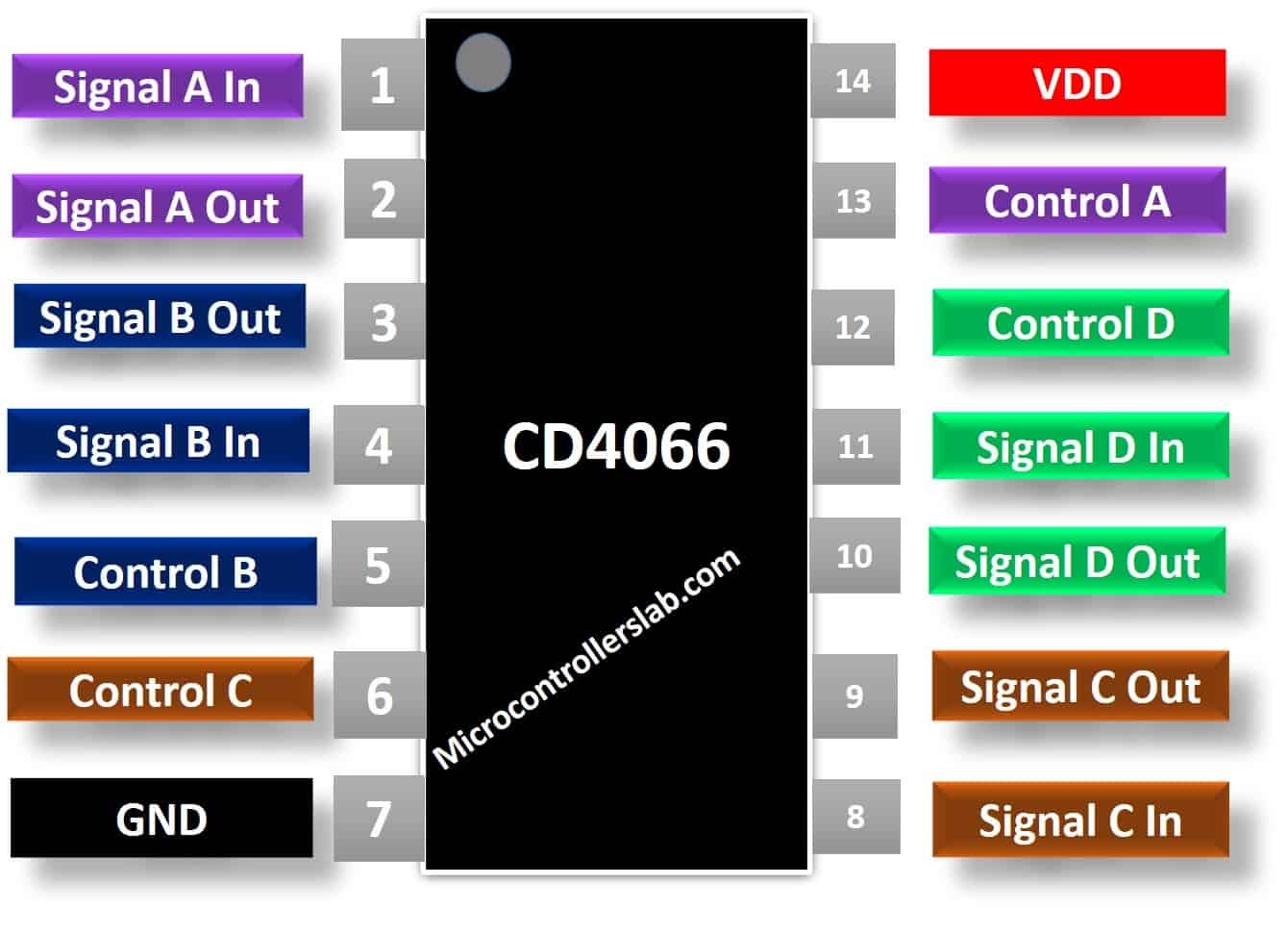
The pinout diagram of CD4066 shows that it consists of fourteen pins. Four bilateral switches have one control signal corresponds with them. The control signal provides a biasing signal to switches.
Pin Configuration Details
This section provides details of each pin and its functionality. Tables list the CD4066 IC pins along with its Pin configuration. This IC has 14 pins in total. Each pin, its name, and description are given in the table below:
| Pin Number | Pin Name | Description |
|---|---|---|
| 1, 4, 8, 11 | IN/OUT SIG A, B, C, | Input/ Output pin for Switch A, B, C and D |
| 2, 3, 9, 10 | OUT/IN SIG A, B, C, D | Output/ Input pin for Switch A, B, C and D |
| 7 | Vss | Ground of the circuit. |
| 14 | Vdd | Voltage Supply |
| 5 | CONTROL_B | switch-B Control input |
| 6 | CONTROL_C | switch-C Control input |
| Pin 12 | CONTROL_D | switch-D Control input |
| Pin 13 | CONTROL_A | switch-A Control input |
CD4066 Features
- Wide voltage supply range of 3V to 15V and maximum switching voltage is 20V
- Wide range of digital (15V) and Peak to Peak analog switching (±7.5 V)
- A high Output current of -0.4mA
- Control pin Voltage at low level is 0.9V (max) and at high level is 11V (min @ 15V Vcc)
- Noise immunity 0.45 VDD (typ.)
- High Output-Voltage Ratio of 80 dB typically at fis = 10 kHz, RL = 1 kΩ
- Very Low Internal Resistance
- Crosstalk between switches is –50 dB at fis = 8 MHz and RL = 1 kΩ which is very low
Where to use CD4066?
CD4066 can be used in multiplexing of analog or digital signals. The switches inside this IC have very low internal resistance. Therefore, it can be used in audio applications and in isolating signals. The advantage of using this IC is that it’s ON impedance is constant over the full input voltage range and the swings in a peak input voltage is equal to the full supply voltage as compared to other single-channel switches.
How to use it?
The working principle of this quad bilateral switch is very easy. The CD4066 IC consists of four switches. It can switch analog signals through digital control. An analog signal is applied at the input of the switch. If a HIGH or 1 value is fed into the control input, the analog signal will be passed from input to the output of a switch. The internal structure of this IC is shown in the figure below.
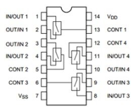
As it is a bilateral switch, therefore it can operate in both directions forward and reverse. Each switch has two pins which can be used as both input and output for switching voltages. Pin 14 is connected to the positive terminal of voltage supply and pin 7 is connected to the ground of the circuit. When the control input is HIGH or 1, the terminals of the switch have low impedance between them, and they are said to be in ON condition. When this input is LOW or 0, the switch is OFF, and the terminal is connected by High impedance.
Truth Table Working Output
The truth table indicating the effect on output by changing inputs is shown in the table given below.
| INPUTS | OUTPUT | |
|---|---|---|
| IN/OUT Signal | Control input | OUT/IN Signal |
| High | High | High |
| 0 | 1 | 1 |
| X | 0 | High Impedance/ switch OFF |
CD4066 Example Circuits
This section contains example circuits and proteus simulations. We design simulation circuits to get a better understanding of CD4066 quad bilateral switches.
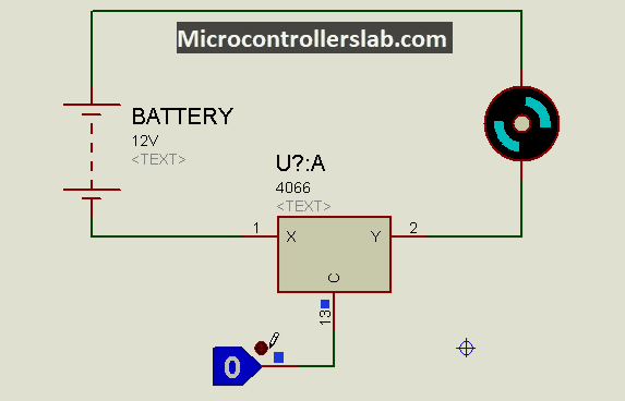
Single Switch Example
In this example, we connect a dc motor with the switch and 12 volts battery to drive this motor. But remember, we can only connect a battery source between 5-18 volts. This is according to the voltage operating range of CD4066.
As you can see from the simulation diagram, motor remains in an off state when there is no control signal. But as soon as we apply a logic high control signal to a control pin of switch A, the motor starts to move. Therefore, the basic purpose of using this ic is to isolate the control signal from the power signal. However, we can also use this IC as a 4×1 multiplexer.
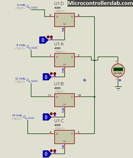
CD4066 Multiplexer Example
This is a 4×1 Multiplexer circuit based on CD4066. Multiplexer gives one output depending on the active selection line. 4×1 multiplexer has four selection lines and one output. Therefore, to design it with this IC, we connect all output pins to a common point. All control pins act as a selection line.
For demonstration purposes, we connect four control pins with different levels of dc voltages such as 4, 8, 12 and 14 volts. Consequently, the voltage associated with the respective control pin ( selection line in this case) will appear at the output of the multiplexer.
CD4066 Quad Bilateral Switch IC Applications
It has a huge array of applications. Some of them are in:
- Switching and multiplexing of Analog Signals and Digital Signals
- Sample and Hold circuits
- Signal Gating, Modulators, Demodulators, Choppers, Commutating Switches
- Dead band filter
- Logic Implementation of Transmission-Gates
- Switching of networks
- Squelch control
- Conversion of Analog-to-Digital and Digital-to-Analog signals
- Digital Control of Frequency, Phase Impedance and Analog-Signal Gain
- CMOS logic implementation
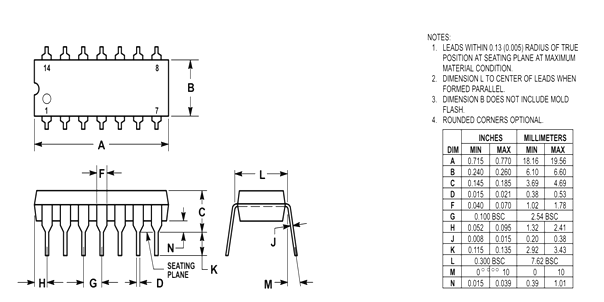
2D Dimension Diagram
CD4066 DataSheet
In conclusion, we can always refer to a datasheet for further information. In addition, we can also check 2D dimension diagrams of other packages for PCB designing.
Hi,
I’ve a CD4066BM to simulate a push on a button with a arduino GPIO.
I when I try to connect OUT1/IN1 on my chip with the button only it seems that the switch is ON. And Vcc, Vss and ControlPin 1 are not yet connected with the Arduino Board.
I my understanding I was expected in that case that the switch should be OFF. Do you have a idea why the switch is ON is that case ?
BR
try to put a 10k ohm resistor between gnd and the gpio of the arduino