The CD4068 is an 8-Input NAND/AND Gate CMOS logic-based IC belonging to a CD4000 series of integrated circuits. Firstly, Two output options are available such as AND and NAND gate. Secondly, the same input pins deliver both logical functions. It is available in a variety of packages which includes 14-pin PDIP, GDIP, PDSO. The typical operating voltage of the IC is +5V, but it can also be operated +10V and +15V. It has a standard symmetric output. This IC is useful for applications requiring low power. Furthermore, it offers a wide voltage operating range.
Recommended Components
The following parts are used in this article, along with a generic electronics kit that is handy for building and testing the circuit.
| Component | How it’s used | Buy on Amazon |
|---|
| CD4068 8-input NAND/AND gate | The CD4068 8-input NAND/AND gate IC this article covers. | Check Price |
| Electronic component assortment kit (1390 pcs) | A handy assortment of resistors, capacitors, LEDs, diodes and transistors for building circuits. | Check Price |
| Digital multimeter (AstroAI) | Measures voltage, current, resistance and checks continuity while you build and debug. | Check Price |
| Breadboard | Solderless base for prototyping the circuit. | Check Price |
| Jumper Wires | Make the connections on the breadboard. | Check Price |
As an Amazon Associate we earn from qualifying purchases. Prices and availability are accurate as of the date/time indicated and are subject to change.
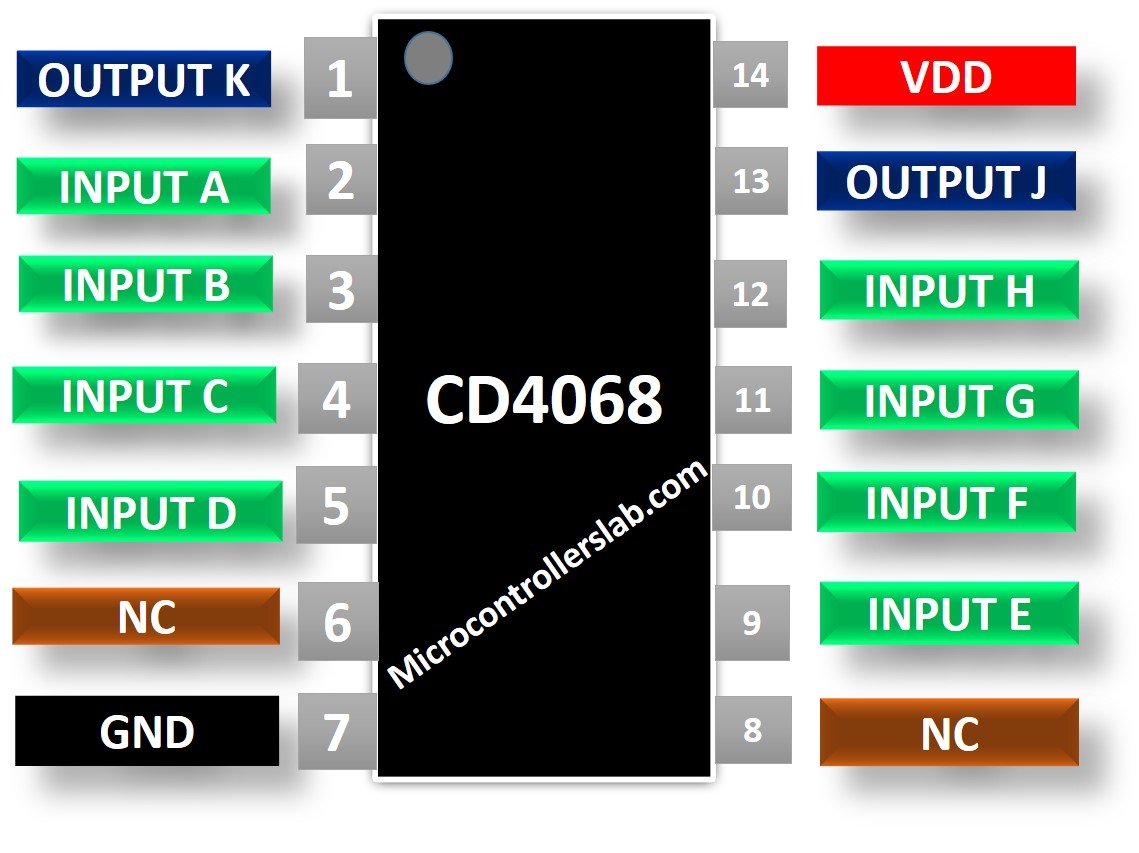
CD4068 Pinout Diagram
This is a CD4068 Pinout diagram 8-bit NAND Gate. Output pins J and K are for NAND and AND gates respectively.

Pin Configuration Details
This IC has 14 pins in the total whose description along with their names and numbers are mentioned in the table given below:
| Pin Number | Pin Name | Description |
| 2, 3, 4, 5, 9, 10, 11, 12 | A, B, C, D, E, F, G, H | Input Data pins |
| 1 | K | Output of AND gate |
| 13 | J | Output of NAND gate |
| 6, 8 | NC | Not Connected |
| 7 | Vss | Negative terminal of voltage supply |
| 14 | VDD | Positive terminal of voltage supply |
CD4068 Features
- 8-input NAND/AND Gate with buffered inputs and outputs
- Operates at medium speed with propagation delay = 75ns at VDD = 10V
- Operating Voltage: 3V to 18V
- Output current range is from -1.5mA to 1.5mA
- Input current over full package temperature range for 18V is 1µA whereas for same voltage but 25°C temperature it is 100nA
- Operating Temperature range is -55 to 125°C
- High Voltage Type (20V Rating) with wide voltage supply range from 3V to 18V
Alternative AND/NAND ICs
74LS00,
CD4011,
74LS08Where and How to Use it?
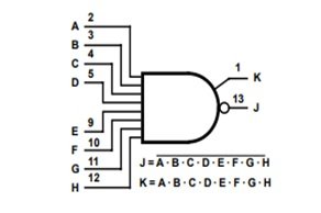
CD4068 can be used for applications that require both NAND and AND gate along with a wide operating voltage range. This IC has 8 inputs and 2 inputs as shown in the logic diagram. The output J is for NAND gate and can be found out theoretically by:
J=(A.B.C.D.E.F.G.H)
The output K is for AND gate. Its value can be mathematically calculated as:
K=~(A.B.C.D.E.F.G.H)

The AND gate gives only HIGH value when all its inputs are HIGH whereas the NAND gate behaves in the opposite manner. It gives LOW value when all its inputs are HIGH. The truth table showing the effect on outputs on applying different values at inputs is given below where 1 stand for HIGH value, 0 stands for LOW value and X stands for it can be HIGH or LOW.
Truth Table of NAND/AND Gates
| DATA INPUTS | DATA OUTPUTS |
|---|
| A | B | C | D | E | F | G | H | J | K |
| 0 | X | X | X | X | X | X | X | 1 | 0 |
| X | 0 | X | X | X | X | X | X | 1 | 0 |
| X | X | 0 | X | X | X | X | X | 1 | 0 |
| X | X | X | 0 | X | X | X | X | 1 | 0 |
| X | X | X | X | 0 | X | X | X | 1 | 0 |
| X | X | X | X | X | 0 | X | X | 1 | 0 |
| X | X | X | X | X | X | 0 | X | 1 | 0 |
| X | X | X | X | X | X | X | 0 | 1 | 0 |
| 1 | 1 | 1 | 1 | 1 | 1 | 1 | 1 | 0 | 1 |
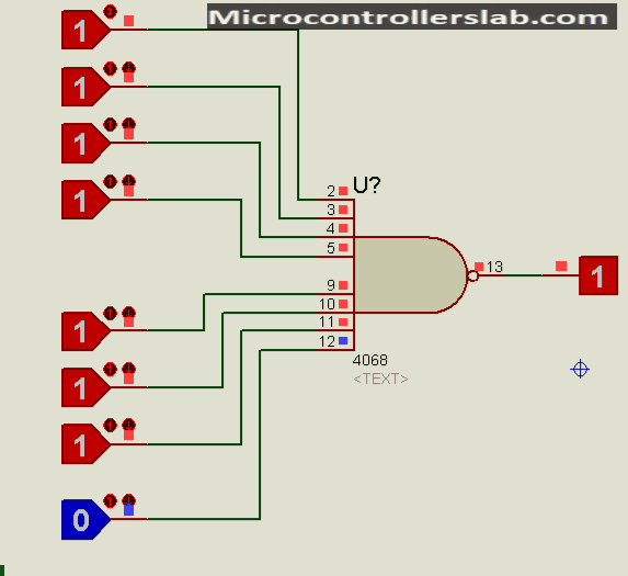
Example Circuit CD4068
To use CD4068 IC all you need to do is to power the IC by connecting a positive terminal of power supply with Vdd and negative terminal or Ground with Vcc. Then apply digital input signals at the input pins and you will get output based on the inputs applied. The output voltage level depends on the power supply. See this proteus simulation:

Applications CD4068 NAND/AND
Some of the applications of CD4068 IC are:
- Logic Buffer circuits can also be designed using this IC
- Combinational Logic Circuits as they are made up of NAND, AND and other basic gates.
- Designing of Encoders and Decoders using a combination of NAND and gates.
- Implementation of Multiplexers and De-multiplexers using this IC.
- Designing of Oscillator circuits, networking, and Digital Systems
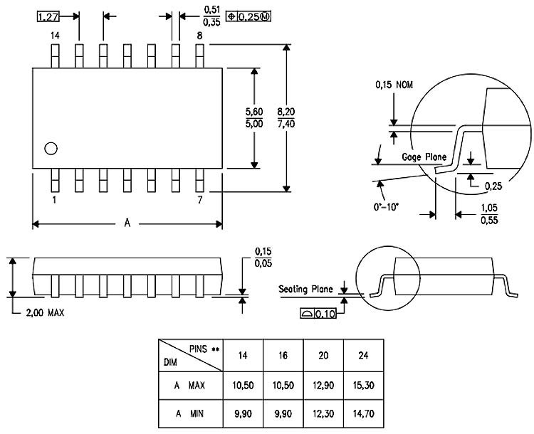
2D Diagram
When we use electronics components in our project, we also need to design a PCB. While designing PCB, the 2D dimension diagram plays an important role. This picture shows a 2D diagram of the CD4068 DIP Package. Download datasheets for other packages.

Download DataSheet
CD4068 Datasheet
 The AND gate gives only HIGH value when all its inputs are HIGH whereas the NAND gate behaves in the opposite manner. It gives LOW value when all its inputs are HIGH. The truth table showing the effect on outputs on applying different values at inputs is given below where 1 stand for HIGH value, 0 stands for LOW value and X stands for it can be HIGH or LOW.