This STM32F4 Discovery Board DAC tutorial shows you how to configure the onboard Digital-to-Analog Converter (DAC) of the STM32F407VG microcontroller using the HAL DAC driver in Keil uvision IDE and generate real analog waveforms on the board’s output pins. The DAC is the inverse of the ADC you learned about in the previous tutorial — instead of converting an analog voltage into a digital number, the DAC converts a 12-bit digital number into an analog voltage between 0 V and 3.3 V. This lets the STM32F4 Discovery Board directly drive analog outputs like audio signals, control voltages, function generator waveforms, and sensor emulation.
In this guide we will use the DAC in its simplest mode — manual software updates, no DMA, no external trigger — so you can see the fundamentals clearly. In follow-up tutorials we will add DMA and timer triggers to generate high-speed, precisely-timed waveforms without CPU overhead.
Recommended Components
The following components are used in this project or are helpful for getting started with STM32F4 Discovery board development.
| Component | How it’s used in this project | Buy on Amazon |
|---|---|---|
| STM32F4 Discovery Board | The STM32F407VG Discovery development board used in this project. | Check Price |
| Mini-USB Cable | Type-A to Mini-B cable to program and power the board over its onboard ST-Link. | Check Price |
As an Amazon Associate we earn from qualifying purchases. Prices and availability are accurate as of the date/time indicated and are subject to change.
What You Will Learn
- What a DAC (Digital-to-Analog Converter) is and how it works internally (R-2R ladder)
- The mathematical formula that relates a DAC input code to the output voltage
- How many DAC channels the STM32F4 Discovery Board has and which GPIO pins they are on
- How to calculate DAC resolution and the minimum step voltage
- The role of
DAC_HandleTypeDefandDAC_ChannelConfTypeDefin HAL DAC configuration - How to select DAC trigger sources (software, timers, external interrupts) and the output buffer
- A complete working example that generates a triangle wave on PA5 using DAC channel 2
- How to observe the DAC output on an oscilloscope
- Common DAC troubleshooting issues and best practices
Prerequisites and Required Components
- STM32F4 Discovery Board (STM32F407G-DISC1)
- Mini USB cable for programming and power via the onboard ST-LINK/V2
- Keil uvision IDE with the STM32F4 device pack installed
- Oscilloscope (or USB logic analyzer with analog input) to view the analog output — without one you won’t be able to see the waveform
- Familiarity with earlier tutorials in this STM32F4 series: LED blinking, push button input, and the ADC tutorial
STM32F4 DAC Introduction
A Digital-to-Analog Converter is a device that converts a digital numeric value into a proportional analog voltage. Unlike an ADC, which turns a continuous voltage into a number, a DAC takes a number and produces a continuous voltage. The analog output depends on two things: the reference voltage (Vref) and the digital value written into the DAC register. As the block diagram below shows, the DAC takes a digital input and a Vref-to-GND reference, and produces a single analog output.
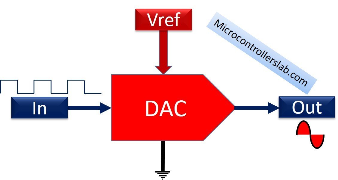
The DAC modules inside the STM32F4 are R-2R ladder based. That’s the same architecture you would find in dedicated DAC chips like the DAC7715, and it gives a monotonic output (increasing digital codes always increase the analog voltage) with good linearity. The formula that relates the digital code D to the analog output is:
Vout = (Vref x D) / 2^N
Where N is the bit width of the DAC. The STM32F407VG DAC is 12-bit, so N = 12 and 2^N = 4096. For more background on DAC types, see our deep-dive article:
DAC Modules on the STM32F4
The STM32F4 Discovery Board is built around the STM32F407VG microcontroller, which has two independent 12-bit DAC channels sharing one DAC peripheral — usually referred to as DAC channel 1 and DAC channel 2 (sometimes also called DAC1 and DAC2). The two channels can be used independently, or in synchronized dual-mode to generate stereo signals, I/Q pairs, or complementary waveforms.
DAC Output Pins on the STM32F4 Discovery Board
On which GPIO pins does the STM32F4 output its DAC signals? Looking at Table 7 in the STM32F407VG datasheet pinout section, the DAC channels are fixed to two specific pins:
- DAC channel 1 → DAC_OUT1 → PA4
- DAC channel 2 → DAC_OUT2 → PA5
When you configure PA4 or PA5 as analog and then start the DAC, those pins stop being GPIO pins and become direct analog outputs. A small warning: on the STM32F4 Discovery Board PA5 is also connected to the onboard MEMS accelerometer’s SCK pin via SPI1 — if you want to use both the DAC and the accelerometer, use DAC channel 1 on PA4 instead.
Calculating the Analog Output from a Digital Input Value
Let’s work through the DAC output equation in practice:
Vout = (Vref x D) / 2^N
The reference voltage Vref is the analog reference pin voltage, which on the STM32F4 Discovery Board is tied to 3.3 V. So the full-scale DAC output range is 0 V to 3.3 V.
Note: The output is bounded by Vref. You cannot get an output above 3.3 V no matter what digital code you write. If you need larger voltage swings, use an external op-amp to buffer and amplify the DAC output.
The STM32F4 DAC is 12-bit, but you can effectively use it as 8-bit by writing 8-bit-aligned values, which some audio applications find convenient. With a 12-bit DAC and D = 1000:
For 12-bit DAC = 2^12 = 4096
Vout = (Vref x D) / 2^N = (3.3 x 1000)/4096 = 0.806V
The digital code D can be any integer between 0 and 4095. The output voltage sweeps between 0 V (D = 0) and approximately 3.29 V (D = 4095 — just below Vref because of the ladder structure).
STM32F4 DAC Accuracy and Minimum Step Voltage
The precision of any DAC is governed by its bit width and reference voltage. For the 12-bit STM32F4 DAC with Vref = 3.3 V, the smallest voltage change the DAC can produce — the least significant bit (LSB) step — is:
Minimum Step Voltage= (Vref x D) / 2^N = (3.3 x 1)/4096 = 0.8mV
So every increment of the DAC input code produces a 0.8 mV change at the output. This is often called the DAC’s resolution and is the same value we calculated for the ADC in the previous tutorial — because both peripherals are 12-bit referenced to the same 3.3 V rail.
HAL DAC Driver on the STM32F4
Now let’s move from theory to code. This section walks through the STM32 HAL DAC library for the STM32F407VG microcontroller.
Two HAL C structures do most of the work: DAC_HandleTypeDef and DAC_ChannelConfTypeDef.
DAC_HandleTypeDef represents the DAC peripheral itself — it holds a pointer to the DAC register block, the state, DMA handles, and error codes:
typedef struct
{
  DAC_TypeDef     *Instance;     /*Pointer to DAC base address discriptor  */
__IO HAL_DAC_StateTypeDef   State;     /*DAC communication state */
  HAL_LockTypeDef     Lock;          /* DAC locking object */
  DMA_HandleTypeDef     *DMA_Handle1;  /*Pointer to DMA handler for channel 1 */
  DMA_HandleTypeDef    *DMA_Handle2;  /*!< Pointer to DMA handler for channel 2 */
  __IO uint32_t         ErrorCode;     /*< DAC Error code*/
}DAC_HandleTypeDef;
In this tutorial we will only use the Instance member. The rest come into play in later tutorials when we add DMA.
Instance: a pointer to the DAC register base. For the STM32F4, there is a single DAC peripheral that hosts both channels, so we simply pass DAC (the register block pointer defined in the STM32 header files).
DAC Channel and Trigger Event Selection
The second important HAL C struct is DAC_ChannelConfTypeDef. It configures one specific DAC channel — trigger source and output buffer behaviour:
typedef struct
{
uint32_t DAC_Trigger; /*Selects the external trigger for the selected DAC channel.
 */
uint32_t DAC_OutputBuffer;  /*Specifies whether the DAC channel output buffer is enabled or disabled. */
}DAC_ChannelConfTypeDef;
DAC_Trigger selects what event causes the DAC to update its output. Possible sources include software triggers, timer TRGO outputs, and external interrupt lines. If you set DAC_TRIGGER_NONE, the DAC updates immediately whenever you call HAL_DAC_SetValue() — which is exactly what we want for this manual-mode tutorial. The other trigger sources become useful when you need precisely-timed updates (for audio, signal generation, or control loops).
The full list of trigger options:
| Value | Function |
|---|---|
| DAC_TRIGGER_NONE | Conversion is automatic and not by external any trigger ( manual) |
| DAC_TRIGGER_T2_TRGO | TIM2 TRGO selected as external conversion trigger for DAC channel |
| DAC_TRIGGER_T4_TRGO | TIM4 TRGO selected as external conversion trigger for DAC channel |
| DAC_TRIGGER_T5_TRGO | TIM5 TRGO selected as external conversion trigger for DAC channel |
| DAC_TRIGGER_T6_TRGO | TIM6 TRGO selected as external conversion trigger for DAC channel |
| DAC_TRIGGER_T7_TRGO | TIM7 TRGO selected as external conversion trigger for DAC channel |
| DAC_TRIGGER_T8_TRGO | TIM8 TRGO selected as external conversion trigger for DAC channel |
| DAC_TRIGGER_EXT_IT9 | EXTI Line9 event selected as external conversion trigger for DAC channel |
| DAC_TRIGGER_SOFTWARE | Conversion started by software trigger for DAC channel |
DAC_OutputBuffer enables or disables the internal output buffer. With the buffer enabled the DAC can drive loads down to about 5 kΩ — which is what you usually want for driving real-world circuits. With the buffer disabled, the output can reach Vss and Vref more accurately (better rail-to-rail behaviour) but can only drive very high-impedance loads. Use DAC_OUTPUTBUFFER_ENABLE unless you have a specific reason to disable it.
| Value | Functions |
|---|---|
| DAC_OUTPUTBUFFER_ENABLE | Enable DAC Buffer |
| DAC_OUTPUTBUFFER_DISABLE | Disable DAC Buffer |
DAC Initialization and Configuration Functions
Two HAL functions handle initialization: HAL_DAC_Init() and HAL_DAC_ConfigChannel().
HAL_StatusTypeDef HAL_DAC_Init(DAC_HandleTypeDef* hdac)The input argument is a pointer to a DAC_HandleTypeDef instance; the return type is HAL_StatusTypeDef:
typedef enum
{
  HAL_OK       = 0x00U,
  HAL_ERROR    = 0x01U,
  HAL_BUSY     = 0x02U,
  HAL_TIMEOUT  = 0x03U
} HAL_StatusTypeDef;
HAL_StatusTypeDef HAL_DAC_ConfigChannel(DAC_HandleTypeDef* hdac, DAC_ChannelConfTypeDef* sConfig, uint32_t Channel)HAL_DAC_ConfigChannel() applies per-channel settings to a specific DAC channel. The first two arguments are pointers to the handle and channel-config structs you just filled in. The third argument selects the channel:
| Value | Function |
|---|---|
| DAC_CHANNEL_1 | Selects DAC channel 1 (output on PA4) |
| DAC_CHANNEL_2 | Select DAC channel 2 (output on PA5) |
As mentioned earlier, in this tutorial we will run the DAC manually — no DMA, no trigger source. Three HAL functions drive manual-mode DAC: HAL_DAC_Start(), HAL_DAC_Stop(), and HAL_DAC_SetValue().
DAC Start, Stop, and SetValue Functions
After initialization, start DAC output with HAL_DAC_Start(). The first argument is the handle pointer, the second is the channel. HAL_DAC_Stop() mirrors this to disable the channel.
HAL_StatusTypeDef HAL_DAC_Start(DAC_HandleTypeDef* hdac, uint32_t Channel);
HAL_StatusTypeDef HAL_DAC_Stop(DAC_HandleTypeDef* hdac, uint32_t Channel);
Once the DAC is started, you set the output voltage by writing a new digital code using HAL_DAC_SetValue():
HAL_StatusTypeDef HAL_DAC_SetValue(DAC_HandleTypeDef* hdac, uint32_t Channel, uint32_t Alignment, uint32_t Data);
The first two arguments are the handle and channel. The third is the data alignment, which tells the DAC how to interpret the value you are writing — 12-bit right-aligned (DAC_ALIGN_12B_R) is what you want in almost every case:
#define DAC_ALIGN_12B_R                    0x00000000U
#define DAC_ALIGN_12B_L                    0x00000004U
#define DAC_ALIGN_8B_R                     0x00000008U
The fourth argument is the numeric value (0–4095 for 12-bit) that will appear as an analog voltage on the DAC output pin.
Last, you must also configure the corresponding GPIO pin (PA4 or PA5) as an analog pin, just like we did for ADC inputs. If you need a refresher on GPIO configuration, see these earlier tutorials:
- LED Blinking Tutorial STM32F4 Discovery Board
- Use Push Button to Control LEDs of STM32F4 Discovery Board
- ADC STM32F4 Discovery Board
STM32F4 DAC Triangle Wave Example Code
The following code generates a triangle waveform on pin PA5 (DAC channel 2) of the STM32F4 Discovery Board. It works by writing increasing 12-bit codes to the DAC (ramp up from 0 V to ~3.3 V), then decreasing codes (ramp down back to 0 V), in an endless loop. The result is a triangle wave whose frequency is determined by the delay in the loop — longer delays mean slower waves.
/*Include header file for STM32F4 HAL libraries and callback functions */
#include "stm32f4xx_hal.h"

/* Function prototype to configure and initialize DAC and GPIO pin */
void configure_DAC(void);
void configure_GPIO(void);
void Delay_ms(volatile int time_ms);
/* create an instance to DAC_HandleTypeDef C struct */
DAC_HandleTypeDef DAC_Config;


/* main function to set DAC numeric value */
int main(void)
{
configure_DAC(); // call DAC initialization and configuration routine
configure_GPIO(); // call GPIO PA5 initialization and configuration routine

/* Start DAC conversion with DAC_CHANNEL_2 */
HAL_DAC_Start(&DAC_Config, DAC_CHANNEL_2);
while(1)
{
	int D_Value = 1;
 while(D_Value < 4000) {
 HAL_DAC_SetValue(&DAC_Config, DAC_CHANNEL_2, DAC_ALIGN_12B_R, D_Value);
 Delay_ms(1);
 D_Value+=100;
 }

 while(D_Value > 1) {
 HAL_DAC_SetValue(&DAC_Config, DAC_CHANNEL_2, DAC_ALIGN_12B_R, D_Value);
 Delay_ms(1);
 D_Value-=100;
 }
 }
}

/* Initialize and configure DAC_Channel_2 */
void configure_DAC(void)
{
 DAC_ChannelConfTypeDef Channel_Config;
 __HAL_RCC_DAC_CLK_ENABLE();
 /* DAC Initialization */
 DAC_Config.Instance = DAC;
 HAL_DAC_Init(&DAC_Config);

 /* DAC channel_OUT2 config */
 Channel_Config.DAC_Trigger = DAC_TRIGGER_NONE;
 Channel_Config.DAC_OutputBuffer = DAC_OUTPUTBUFFER_ENABLE;
 HAL_DAC_ConfigChannel(&DAC_Config, &Channel_Config, DAC_CHANNEL_2);
}
/* Initialize and configure GPIO PA4 as a analog pin */
void configure_GPIO(void)
{

/* DAC GPIO ---> PA5 */
 GPIO_InitTypeDef GPIO_InitStruct;
 GPIO_InitStruct.Pin = GPIO_PIN_5;
 GPIO_InitStruct.Mode = GPIO_MODE_ANALOG;
 GPIO_InitStruct.Pull = GPIO_NOPULL;
 HAL_GPIO_Init(GPIOA, &GPIO_InitStruct);
}
/*Generate ms */
void Delay_ms(volatile int time_ms)
{
	      int j;
        for(j = 0; j < time_ms*4000; j++)
            {}  /* excute NOP for 1ms */
}
DAC Example Code Output
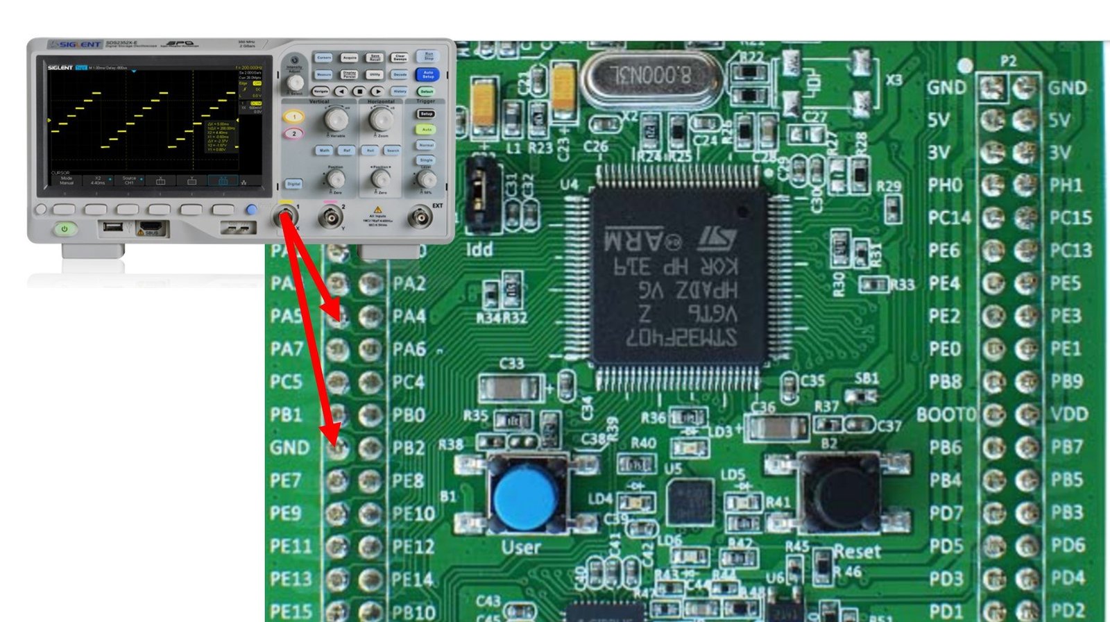
To see the generated waveform, connect the positive probe of an oscilloscope to PA5 on the STM32F4 Discovery Board and the oscilloscope ground to one of the board’s GND pins. Build and flash the project. You should see a triangular waveform sweeping between 0 V and ~3.3 V on the oscilloscope screen.
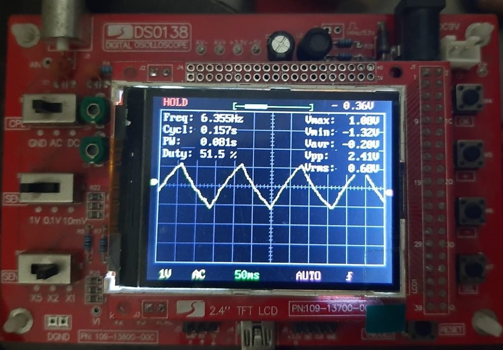
How the Triangle Wave Code Works
Generating a triangle wave is just two ramps glued together. The first inner while loop writes ever-increasing codes from 1 up to 4000, in steps of 100, with a 1 ms delay between each write. This produces the rising edge of the triangle.
int D_Value = 1;
 while(D_Value < 4000) {
 HAL_DAC_SetValue(&DAC_Config, DAC_CHANNEL_2, DAC_ALIGN_12B_R, D_Value);
 Delay_ms(1);
 D_Value+=100;
 }
Once D_Value reaches 4000, the first loop exits and the second loop takes over — writing decreasing codes from ~3900 down to 100 in steps of 100. That produces the falling edge. Then the outer while(1) runs the sequence again, indefinitely, producing a continuous triangle wave.
 while(D_Value > 1) {
 HAL_DAC_SetValue(&DAC_Config, DAC_CHANNEL_2, DAC_ALIGN_12B_R, D_Value);
 Delay_ms(1);
 D_Value-=100;
 }
To change the waveform shape, replace the ramp loops with a lookup table of samples (for sine waves) or use a counter modulo some period (for square and sawtooth). To make the wave faster, reduce the Delay_ms(1) delay or increase the step size. In the coming tutorials we will use DMA + timers to generate smooth, high-frequency waveforms without any CPU involvement.
Troubleshooting STM32F4 DAC Issues
- No output on PA4 or PA5. Most likely the DAC clock is not enabled. Add
__HAL_RCC_DAC_CLK_ENABLE()beforeHAL_DAC_Init(). Also make sure the GPIO pin is set toGPIO_MODE_ANALOG. - Output stuck at 0 V or 3.3 V. If you are using
DAC_OUTPUTBUFFER_ENABLE, the buffer has some headroom from the rails — the true minimum is around 0.2 V and the maximum is around 3.1 V. Disable the buffer for true rail-to-rail output (at the cost of drive capability). - Waveform is distorted or stepped. Your update rate is too low compared to the frequency you are trying to produce. Either reduce the software delay or switch to DMA + timer triggering for high-quality waveforms.
- Output voltage is lower than expected. You are driving a low-impedance load through the buffer. The internal buffer can drive loads down to ~5 kΩ — anything lower pulls the output voltage down. Use an external op-amp buffer.
- DAC channel 2 interferes with the accelerometer. On the STM32F4 Discovery Board, PA5 is shared with SPI1_SCK going to the MEMS accelerometer. If you need both, use DAC channel 1 on PA4 instead.
- Noisy analog output. Make sure VDDA is filtered and connected to 3.3 V (the Discovery Board does this correctly by default). Keep DAC output wires short, and add a small capacitor (100 pF–1 nF) from the output pin to ground for simple RC smoothing.
Frequently Asked Questions
How many DAC channels does the STM32F4 Discovery Board have?
The STM32F407VG microcontroller provides two independent 12-bit DAC channels. DAC channel 1 outputs on PA4 and DAC channel 2 outputs on PA5. Both channels can be used simultaneously for stereo audio or dual-waveform applications.
What is the maximum output voltage of the STM32F4 DAC?
Maximum DAC output equals Vref+ — on the STM32F4 Discovery Board that’s 3.3 V. The output cannot exceed Vref. If you need larger voltage swings, use an external op-amp amplifier or a boost stage.
Can I generate a sine wave with the STM32F4 DAC?
Yes. Create a lookup table of sine samples (e.g., 64 or 256 points) that span 0 to 4095, then write them sequentially to the DAC inside a timed loop. For stable, high-frequency sine generation, drive the DAC from DMA triggered by a timer — that keeps the update rate precise without CPU jitter.
What is the difference between DAC output buffer enabled and disabled?
With the output buffer enabled, the DAC can drive moderate loads (down to about 5 kΩ) but sacrifices a bit of rail-to-rail range. With the buffer disabled, the DAC is effectively connected to the R-2R ladder directly — output reaches 0 V and Vref more precisely, but can only drive very high-impedance loads without sagging. Most beginners should leave the buffer enabled.
Why is my DAC output not reaching exactly 3.3 V?
Two reasons. First, because of the 12-bit R-2R ladder, the maximum code 4095 gives an output of (4095/4096)×3.3 ≈ 3.299 V — just below Vref. Second, with the output buffer enabled, there is some saturation voltage near the rails. If you need the absolute highest voltage, disable the output buffer, but only if your load is high-impedance.
Do I need an oscilloscope to test the STM32F4 DAC?
For waveforms, yes — a multimeter only shows static values, and the triangle wave in this tutorial changes too fast to read on one. As a workaround, you can slow the wave down to 1 Hz or slower and watch a multimeter sweep up and down, or connect the DAC output to an ADC input on the same board and print the values via UART to verify the ramp.
Conclusion
In this STM32F4 DAC tutorial you learned how the STM32F407VG’s two 12-bit DAC channels work, how to configure them with the HAL library, and how to generate a real triangle waveform on PA5. Combined with the ADC knowledge from the previous tutorial, you now have both directions of analog-to-digital and digital-to-analog conversion covered. Next in the series we will look at UART communication on the STM32F4 Discovery Board — the peripheral that lets your firmware talk to a PC, a Bluetooth module, a GPS module, or almost any other serial device.
The code in this article is incomplete and does not compile.
You need to include the complete source listing.