The DAC0832 is a simple and advance TTL device used to convert the 8-bit digital data to an analog signal. It is designed to directly interface with 8080, 8048, 8085, Z80, microcontroller and microprocessor. The IC comes up with special circuitry of resistors which helps to convert the digital signal stepwise to an analog signal. DAC basically converts the digital signal to digital by making the series of input data. CMOS and Logics gates used in DAC to achieve low current levels. Later that TTL logic is used to convert the low current levels to voltage levels.
Recommended Components
The following parts are used in this article, along with a generic electronics kit that is handy for building and testing the circuit.
| Component | How it’s used | Buy on Amazon |
|---|---|---|
| DAC0832 8-bit DAC IC | The digital-to-analog converter IC discussed in this article, 20-pin DIP. | Check Price |
| Electronic component assortment kit (1390 pcs) | A handy assortment of resistors, capacitors, LEDs, diodes and transistors for building circuits. | Check Price |
| Digital multimeter (AstroAI) | Measures voltage, current, resistance and checks continuity while you build and debug. | Check Price |
| Breadboard | Solderless base for prototyping the circuit. | Check Price |
| Jumper Wires | Make the connections on the breadboard. | Check Price |
As an Amazon Associate we earn from qualifying purchases. Prices and availability are accurate as of the date/time indicated and are subject to change.
DAC0832 8 bit DAC Pinout
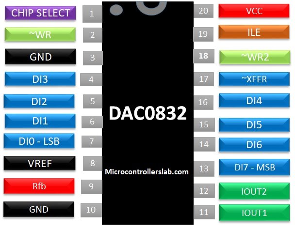
PIN CONFIGURATION OF DAC0832 8-BIT DAC
This table provides the details of all the pins available on DAC0832 IC.
| PINS | DETAIL | |
|---|---|---|
| CS | Pin 1 | CS stands for chip select. It is used in case of multiple DAC; it is used when we need to select which chip circuit will be used at a specific time. CS pin is an active low pin, it should be grounded. |
| WR | Pin 2 | Write pin is used for successfully transfer the data from input latch to DAC latch. It’s an active low pin. |
| GND | Pin 3 | GND pin is a ground pin used as a common ground for digital input data device. |
| DI 3 | Pin 4 | Digital data has a total 8 inputs. Pin 4 will take input 3 from the digital data. |
| DI 2 | Pin 5 | Pin 5 will take digital input 3 for conversion |
| DI 1 | Pin 6 | Pin 6 will take digital input 2 to convert the data. |
| DI 0 | Pin 7 | Pin 7 will take the least significant bit of the input data for conversion. |
| VREF | Pin 8 | Pin 8 will be used as VREF pin. It will describe the DAC max voltages. |
| RFB | Pin 9 | Pin 9 will be used as a feedback resistor. It will use to provide the feedback to the external OP-AMP used to provide voltages to DAC0832. |
| GND | Pin 10 | Pin 10 will also be used as ground like Pin 3. |
| IOUT 1 | Pin 11 | DAC gives output in the current. So, Pin 11 will be used as one current output. |
| IOUT 2 | Pin 12 | Pin 12 is used as the second current output. |
| DI 7 | Pin 13 | Pin 13 is used as a digital input for the Most Significant bit. |
| DI 6 | Pin 14 | Digital input 7 will goes to pin 14 for analog conversion. |
| DI 5 | Pin 15 | Pin 15 will be used as Digital input 6 for analog conversion. |
| DI 4 | Pin 16 | It is used as Digital input 5 for DAC. |
| XFER | Pin 17 | XFER is used as a control signal. It works with the combination of WR pin it is and an active low pin |
| WR2 | Pin 18 | Write is a control pin that works with the combination XFER pin. It enables the input data to transfer from the stored input latch to DAC. It’s an active low state pin. |
| ILE | Pin 19 | It is used as a control signal to make successful input data to store it in the DAC register. It’s an active HIGH state pin |
| Vcc | Pin 20 | Pin 20 is used to apply the power supply to the DAC. |
FEATURES of DAC0832
- DAC0832 has the ability to take the 8-bit digital data input from the controller or any low voltage device.
- The single power supply can be used to operate the DAC0832.
- It doesn’t require any kind of device to interface with any microcontroller. It could be attached directly.
- DAC0832 can be operated using a logic gate. It is not dependent on any microprocessor or any microcontroller.
- Every CMOS and TTL device are compatible with DAC0832.
- It is usable in switching mode for voltages.
- It comes in two packages: SOIC and PLCC with all 20 pins.
- DAC is workable with 10 voltage reference.
- Its linearity is specifying with full scale and zero adjust only. It isn’t best for straight-line fit.
- DAC0832 is interchangeable and fully compatible with 12-bit DAC1230 Series.
- It has high ESD protection of about 800V.
SPECIFICATIONS of DAC
- It has 1us of current settling time.
- It has a voltage range of 5 – 15 DC Volts.
- DAC0832 has low power consumption range is 20mW.
- Maximum power dissipation of DAC is 500mW
- The operating temperature of DAC is 0 to +75 degrees centigrade.
- It only works with 8-bit digital input data.
How to generate an analog signal with DAC0832
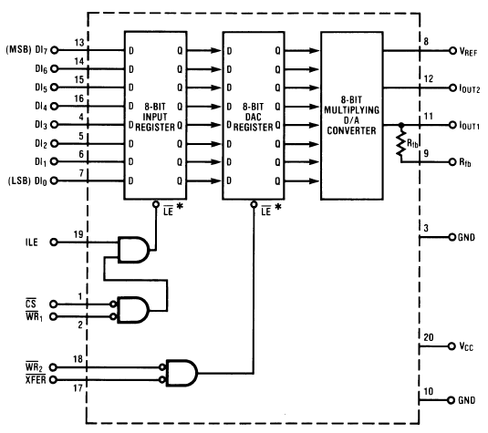
DAC0832 has a simple internal structure. In DAC the 8-bit data has been given to the input register, which is controlled by one AND gate and one NAND gate. The combination of AND & NAND gate will take three input signals, the signals are CS, WR1, and ILE. When CS and WR1 become LOW and ILE becomes HIGH then data transfer from the input register to the 8-bit DAC register. After transferring data into DAC register the data is controlled by a NAND gate which takes input from two pins, which are WR2 and XFER.
The data in DAC Register is replaceable from the previous input register and it could be transferred to DAC Converter. In DAC converter data will be converted to two outputs. The output will be known as the current output. The output will be in a current form which will convert further to the voltage by using the TTL circuit and RFB pin.
Working of DAC0832
To make the DAC fully workable we need to control all 5 control pins. The Pin ILE should be HIGH and other control pins, CS, WR1, WR2, and XFER should be LOW to put DAC in work. The VREF pin will be connected to the power to describe the max output/input voltages. After that, we need an OP-AMP circuit to convert the voltages to current. Here is the circuit we will follow.
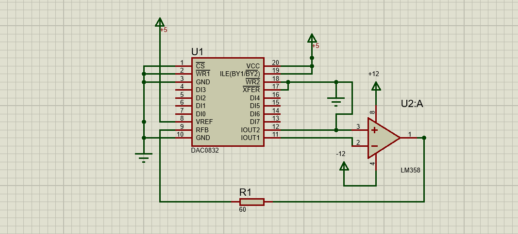
The output pin will be attached to the LM358 OPAMP and they will connect to the DC0832. The Output will be connected to the RFB pin through a 60-ohm resistor. The value of the resistor will be variant according to the circuit. The output voltage will be equal to the power given on VREF. VREF will describe the MAX output voltage. The OPAMP will not only convert the current to voltage. It will also increase the voltage level at the output pin of OP-AMP, that’s why the resistor will be used to get the exact voltages. The voltage will be provided at VCC and ground will be provided at GN pin. The Controls pin will be grounded expect ILE. It will need to be HIGH to give the output. The output voltage will be 5V but it will only happen when our digital input is total HIGH.
Example to convert digital into analog with DAC0832
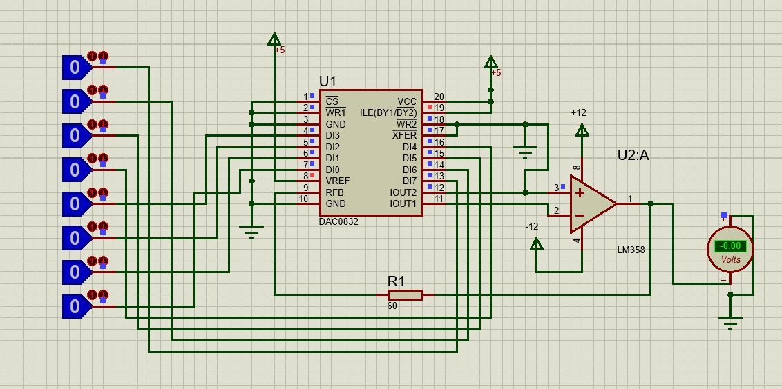
As an example, we will convert the digital signal to voltages. The digital signal will be input through the digital pins in 8-bits and they will give the output in voltage which will be able to detectable through any dc voltmeter. The lowest input value on digital pins will be “00000000” and the maximum input value will be “11111111”.
Converting low logic to analog low signal
When we will give the lowest value as input then it will convert the value to 0 but in case of the maximum input value, the output will be maximum voltages of VREF pins. Due to all pins are HIGH the data will be considered as maximum output. IC is unable to understand how to convert binary to analog data, so it will give us the output by considering VREF. To do this Example design the following circuit in your proteus.
Converting digital high logic to analog high signal
The above circuit will be using logic gates to make it understandable for all kind of microcontrollers. When we give the low logic at all digital pins then the output is 0V. Now try giving HIGH at all digital pins.
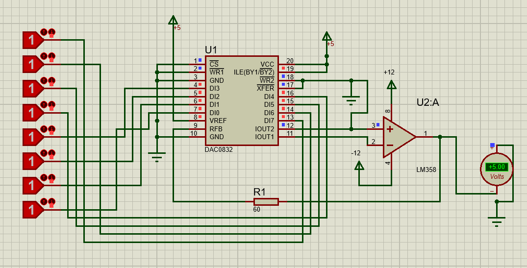
You may notice that when we apply all HIGH logics then output is 5 volts, which is equal to VREF voltages. The output voltages were more than 5V due to the use of OP-AMP conversion. To make it perfect a 60-ohm resistor is used to make the output equal to 5Volt. The size of the resistor will be dependent every time on the power of OP AMP. The value of voltages varies for different powers. The output of multiple DAC0832 can be used for multiple outputs. Then we will need to control the CS pin to make the usage of specific IC at a specific time.
DAC0832 Proteus Simulation
In this simulation, we give a digital input signal with 74LS393 counter and you can see the analog output on digital dc voltmeter.
You may be interested in : DAC0808 8-bit Digital to Analog Converter