What is Double layer PCBs ? Double layer PCBs (otherwise called Double-Sided Plated Thru or DSPT) circuits are the entryway to higher innovation applications. They take into account nearer (and maybe additionally) directing follows by substituting between a best and base layer utilizing vias. Today, double sided printed circuit board innovation is maybe the most mainstream kind of PCB in the business.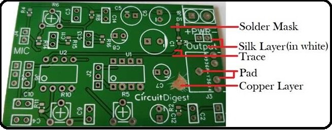
Construction of double layer PCB:
All the components of double layer pcb are explained below:
- Pad: pad is only a bit of copper on which lead of parts are mounted and on which binding are done. Pads gives the mechanical help to the segments.
- Trace In PCB, parts are not associated with the assistance of wires. All parts are associated with a leading material like copper. This copper some portion of PCB which is utilized to associate all segments that is known as follow. Follow is looks like underneath figure.
- Layers: : According to application, cost and accessible space of circuit, client can pick the layer of PCB. Most straightforward in development, simple to plan and most valuable in routine life is single layer PCB. Be that as it may, for vast and complex circuit, twofold layer PCB or Multi-layer PCB is most favored contrasted with single layer PCB. Presently a day, in multi-layer PCB, 10-12 layers can be associated and most basic thing is to convey between the parts in various layer.
- Silk layer: Silk layer is utilized for printing line, content or any workmanship on the surface of PCB. For the most part, for screen printing epoxy ink is utilized. Silk layer can be utilized as a part of best or potentially base layer of PCB as indicated by client necessity which is known as silk screen TOP and silk screen BOTTOM
- Top and bottom layer: In Top layer of PCB, all segments are mounted in this layer of PCB. For the most part, this layer is green shaded. In base layer of PCB, all segments are fastened through the opening and lead of segments is known as base layer of PCB. At some point, in top or potentially base layer PCB is covered with green shading layer, which is known as weld veil.
- Solder Mask: There is one additional layer on the top of copper layer called as Solder Mask. This layer generally has green color but it can be of any color. This insulating layer is used for to prevent accidental contact of pads with other conductive material on PCB.
types of double layer PCBs
here are a few kinds of PCB accessible for the circuit. Out of these kinds of PCB, we need to pick the proper sort of PCB as indicated by our application.
- Single-layer PCB
- Double-layer PCB
- Multi-layer PCB
- Flexible PCB
- Aluminium backed PCB
- Flex-rigid PCB
1) Single Layer PCB:
A single layer PCB is otherwise called single sided PCB. This sort of PCB is straightforward and most utilized PCB in light of the fact that these PCBs are anything but difficult to plan and fabricate. One side of this PCB is covered with a layer of any directing material. By and large, copper is utilized as directing material for PCB, in light of the fact that copper has great leading trademark
2) Double Layer PCB:
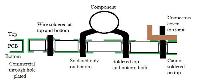
Double layer PCB is otherwise called double layer PCB. As name recommends, in this sort of PCB, a thin layer of directing material, similar to copper is connected to both best and base sides of the board. In PCB, on various layer of board, comprise through, which has two cushions in comparing position on various layers.
3) Multi-Layer PCB:
Multilayer PCB has in excess of two layers. It implies that, this sort of PCB has no less than three conductive layers of copper. For securing the board stick is sandwiched between the layer of protection which guarantees that the abundance warmth won’t harm any part of circuit. This write PCB outlining is extremely mind boggling and utilized as a part of exceptionally confounded and expansive electrical assignment in low space and conservative circuit. This sort of PCB is utilized as a part of vast application like GPS innovation, satellite framework, therapeutic gear, document server and information stockpiling.
4) Flexible PCB:
Flexible PCB is otherwise called Flex circuit. This sort of PCB utilized adaptable plastic material like polymide, PEEK (Polyether ether ketone) or straightforward conductive polyester film. The circuit board is by and large place in collapsed or turned.
5) Rigid PCB:
Rigid PCBs are made out of strong material which don’t permit PCB from winding. Same as flex PCB, Rigid PCB additionally have distinctive layer arrangement like single layer, twofold layer and multi-layer Rigid PCB. State of this PCB isn’t change after establishment.
6) Flex-rigid PCB:
Mix of Flexible circuit and rigid circuit is most vital board. Flex-inflexible sheets comprises of various layers of flexible PCB joined to various unbending PCB layer. Flex-rigid board is as appeared in figure. It is utilized as a part of mobile phones, advanced cameras and cars and so on.
Applications of Double layer PCBs
There are close boundless applications for old and new outlines. Almost negligible difference surface mount, ultra high copper fabricate, high and low temperature, Solder covered, Silver, and Gold completions are only a couple of cases of DSPT applications.Despite the fact that PCBs are regularly connected with PCs, they can be found in numerous other electronic gadgets, for example, TVs, Radios, Digital cameras and Cell telephones. Notwithstanding their utilization in buyer gadgets and PCs, diverse sorts of PCBs are utilized as a part of an assortment of different fields, including:
- Medical devices Gadgets items are presently denser and devour less power than past ages, making it conceivable to test new and energizing restorative innovation. Most restorative gadgets utilize a high-thickness PCB, which is utilized to make the littlest and densest plan conceivable. This lightens a portion of the one of a kind imperatives required with creating gadgets for the medicinal field because of the need of little size and light weight. PCBs have discovered their way into everything from little gadgets, for example, pacemakers, to significantly bigger gadgets like X-beam hardware or CAT check machines.
- Industrial machinery. PCBs are generally utilized as a part of powerful mechanical apparatus. In places where current one-ounce copper PCBs don’t fit the necessities, thick copper PCBs can be used. Cases of circumstances where thicker copper PCBs would be advantageous incorporate engine controllers, high-current battery chargers and modern load analyzers.
- Lighting: As LED-construct lighting arrangements get with respect to in prevalence due to their low power utilization and large amounts of productivity, so too do aluminum-supported PCBs which are utilized to make them. These PCBs fill in as warmth sinks and consider more elevated amounts of warmth exchange than a standard PCB. These same aluminum-upheld PCBs frame the reason for both high-lumen LED applications and fundamental lighting arrangements
- Automotive and aerospace industries Both the car and aviation ventures make utilization of adaptable PCBs, which are intended to withstand the high-vibration conditions that are normal in the two fields. Contingent upon determinations and plan, they can likewise be extremely lightweight, which is a need when producing parts for transportation ventures.
Advantages of double layer PCB
double layer pcb sheets are a typical instrument in both generation and model circuits. They permit a higher thickness in segments and make laying of tracks a simpler procedure.Same as a customary circuit board, Double sided sheets are made with a substrate of non conductive material, over which a layer of copper is set over it, and on account of twofold sided sheets, the copper is additionally layered on the base side of the substrate.Similarly as with a circuit board, there are points of interest to the utilization of one sort over another.Twofold sided sheets, as I said prior, permit a higher thickness of part. This is on account of you have an entire additional layer where you can add tracks to interface the segments, liberating space on the other to put the parts nearer together or include additional associations for IC with high stick checks.
Another favorable position of utilizing twofold sided loads up is the expanded warmth scattering that an additional layer of copper gives, this can be accomplished in the drawing procedure, just expelling enough copper to make the tracks, leaving the additional copper as opposed to evacuating it totally. At the point when to Use Double Sided Boards, The choice to utilize twofold sided sheets should be viewed as painstakingly, due to the additional multifaceted nature underway and treatment of the completed board, and in addition the costs related can make utilizing a twofold sided board a problematic decision to use in an electronic circuit venture.The greatest thought is fabricating costs, in light of the fact that most producers will charge additional setup expenses for preparing the additional side, on carving and soldermask, as well as on part designs included the silkscreen procedure.