LT3750 is a flyback converter which can charge capacitors of any size. This chip uses a patented boundary mode control scheme. This scheme reduces the size of the transformer integrated into chip and losses due to transition. It has a wide range of input voltages and charges high voltage capacitors rapidly and quickly.
Recommended Components
The following parts are used in this article, along with a generic electronics kit that is handy for building and testing the circuit.
| Component | How it’s used | Buy on Amazon |
|---|---|---|
| Electronic component assortment kit (1390 pcs) | A handy assortment of resistors, capacitors, LEDs, diodes and transistors for building circuits. | Check Price |
| Digital multimeter (AstroAI) | Measures voltage, current, resistance and checks continuity while you build and debug. | Check Price |
| Breadboard | Solderless base for prototyping the circuit. | Check Price |
| Jumper Wires | Make the connections on the breadboard. | Check Price |
As an Amazon Associate we earn from qualifying purchases. Prices and availability are accurate as of the date/time indicated and are subject to change.
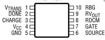
LT3750 Pinout Diagram
This figure shows the pinout diagram of LT3750 capacitor charger IC. We can easily charge 300 volts and three, six and nine ampere capacitors easily. Application example circuit is available at the end of article.
Pin Description
Pin#01 Vtrans: It is the voltage supply for the transformer which provides power to its primary coil and to the internal circuit which detects boundary mode.
Pin# 02 ~Done: It is the open collector pin of an internal transistor which indicates the completion of one charging cycle by turning on the NPN transistor.
Pin# 03: CHARGE It is the charge Pin. On applying high signal at this pin, a new charge cycle will begin. It shut down the internal circuit if applied with a low signal.
Pin#04:Vcc It is the Voltage supply input pin.
Pin#05: GND Connect it directly to main ground of circuit.
Pin#06: SOURCE Connect this pin to the source terminal of NMOS power MOSFET and a resistor which senses the drain current of power MOSFET. The maximum current limit is 78mV/RSENSE.
Pin# 07: GATE It is the gate output of power MOSFET. Connect this pin to gate terminal of power Mosfet.
Pin# 08: RDCM It is a sense pin of LT3750 which senses the discontinuous mode. If the output voltage is below the target value, it starts the new charging cycle when the transformer current decays to zero.
Pin# 09: R It converts the output voltage to current which is proportional to output capacitor voltage.
Pin# 10: RBG It senses the output voltage by sensing the voltage across the RBG resistor and disables charging when its voltage becomes equal to 1.24V.
Features
- LT3750 is a capacitor charger which can charge capacitor of any size.
- Its output voltage is adjustable. You can adjust it using a single resistor.
- The input voltage range Vcc is 3V to 24V.
- It has a 2A MOSFET gate which can drive voltages within VCC – 2V range.
- Under the no-load condition, it provides stable operation.
- The charger has very low noise at the output.
- It can sense primary voltage or output voltage at the secondary side.
- It can also detect Over and Under voltages.
Other equivalent options are LT3751
Where and How to use LT3750?
LT3750 is a capacitor charger controller therefore it is used for charging capacitors. The CHARGE pin provides ON and OFF control to the user and starts a new charging cycle. When the charging value of the capacitor has reached its target value, the ~done pin will send a signal and will stop the charging.
Example Circuit
The figure below shows a circuit for charging 300V, 6A capacitor. Bypass pin1 with a 10µF capacitor and transformer’s primary winding with a large capacitor of 56 µF.
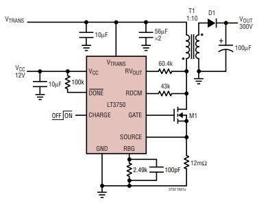
Connect pin2 with a pull-up transistor. It indicates when the output voltage has reached the target value and turns on the built-in NPN transistor. It also turns on the NPN transistor in case of thermal shutdown or Undervoltage lockout. CHARGE pin can enable or disable the lt3750 controller. It will enable the device when applied with 1.1V or greater than 1.1V voltage and disable the device when applied with 0.2V. Bypass input voltage supply by a 10µF ceramic capacitor.
You can adjust the output voltage through turns ratio of transformer and two external resistors. The above circuit can charge a 100µF capacitor within 300 ms to 300V.
LT3750 Applications
Its applications include:
- High Voltage Regulated Supply and a Capacitor Charger
- Professional Photoflash Systems
- Emergency Strobe
- Electric Fences
- Security/Inventory Control Systems
- Detonators