Recommended Components
The following parts are used in this article, along with a generic electronics kit that is handy for building and testing the circuit.
| Component | How it’s used | Buy on Amazon |
|---|---|---|
| Electronic component assortment kit (1390 pcs) | A handy assortment of resistors, capacitors, LEDs, diodes and transistors for building circuits. | Check Price |
| Digital multimeter (AstroAI) | Measures voltage, current, resistance and checks continuity while you build and debug. | Check Price |
| Breadboard | Solderless base for prototyping the circuit. | Check Price |
| Jumper Wires | Make the connections on the breadboard. | Check Price |
As an Amazon Associate we earn from qualifying purchases. Prices and availability are accurate as of the date/time indicated and are subject to change.
MCP16252 Pinout Diagram
The pinout diagram of MCP16252 shows all the pins. It comprises of 8 pins. Due to built-in components for a buck regulator design, we only need a few resistors and capacitors to make it functional. Vouts and Voutp are the output pins.Note : Pinout out for MCP16251/2 for both ICs is the same. In fact, most of the electrical features and specifications are also the same.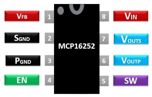
Pin Configuration Details
The detailed description of pins of boost regulator MCP16252 IC is mentioned in the table below.| Pin Number | Pin Name | Description |
|---|---|---|
| 1 | VFB | The feedback input is connected to the resistor divider between output and Ground. It is used to set the output voltage. |
| 2 | SGND | It is the signal ground pin which is normally connected to the ground of the circuit. |
| 3 | PGND | It is the power ground pin and is also connected with the common ground. |
| 4 | EN | Enable is a control input pin. To enable the IC, it is connected to logic HIGH or leave unconnected. Connect it to LOW logic to disable or shut down the IC. |
| 5 | SW | It is the boosting or rectifying switch input used for power switching of external inductor. |
| 6 | VOUTP | This is an output voltage power pin connected externally. |
| 7 | VOUTS | This is an output voltage sense pin and it is also connected externally. |
| 8 | VDD | The input voltage signal is applied at this pin. |
Difference between MCP16252 and MCP16251
All features and electrical specifications are the same for both boost regulators. There is only one difference between them. MCP16252 offers input to output bypass features that MCP16251 does not support. Similarly, later regulators support the true output disconnect that earlier does not have.MCP16252/1 Features
- It can perform the operation of PWM and PFM automatically
- It has one output along with an internal synchronous rectifier, built-in over-temperature protection and anti-ringing control
- PWM operation is performed at 500KHz
- Input Voltage Range is from 0.82V to 5.5V
- Adjustable output voltage range of 1.8V to 5.5V
- It has a very high efficiency of up to 96% (Typically).
Where to use MCP16252 Boost Regulator?
The Mcp16252 IC has a wide range of input and output voltages and a very high efficiency of 96%. It is basically used in applications requiring DC to DC converters powered through one, two or three-cell alkaline, NiCd, NiMH and one-cell Li-Ion or Li-Polymer batteries. You can use this IC in regulated DC power supplies.How to use MCP16252/1?
It requires a minimum number of components to operate. A simple test circuit diagram is shown below. Vin is connected to a battery. Connect pin Vin to the input voltage source to VIN which should be decoupled with a capacitor of value 4.7µF to ground. Enable pin is normally connected to high as it is used for enabling or shutdown of IC. Pins Vouts and Voutp are connected externally to a voltage divider.Example Circuit
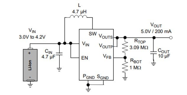 The feedback voltage pin is also connected to this network of resistors and regulates the output voltage through this network. In addition to a voltage divider network, a capacitor is also connected to the output pin for stable voltage. It reduces the ripples during sudden load transients. The value of this capacitor should be large enough so that the time constant value is large and large time constant ensures constant voltage at the output.
How to calculate RTOP and RBOT resistors values?
For a specific output voltage, we can calculate, feedback resistors values. We can use this formula to calculate resistors values:RTOP = RBOT x ( ( Vout/VFB) - 1 )
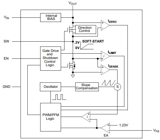
Block Diagram
As you can see from the block diagram that MCP16252 has all components inside the chips. Followings are the main components:- Soft Starter: It provides soft-start by eliminating high in-rush current at the start.
- Gate Driver Circuit
- Oscillator Circuit
- Pulse width modulation Control
- Current sensing and protection
MCP16252 Synchronous Boost Regulator Applications
It is a boost converter used in:- Remote Controllers, Portable Instruments and applications requiring portable devices
- Wireless Sensors and Solar Cell Applications
- regenerative braking of DC motors
- Bluetooth Headsets and devices like digital cameras, smart phones and Mp3 player etc.
- Regulated DC power supplies and distributed power supplies of +3.3V to +5.0V
- Bias for Status LEDs
- Personal Care and Medical Products
2D Diagram
The two-dimensional diagram of its 8 lead TDFN package is given below.