OP07 is a precision operational amplifier IC consisting of a single operational amplifier inside a chip. The OP07 operational amplifier has a slew rate is the rate of 0.3-V/μs. It performs a low noise operation and has a wide input voltage range. It has features of internal frequency compensation and offset nulling.
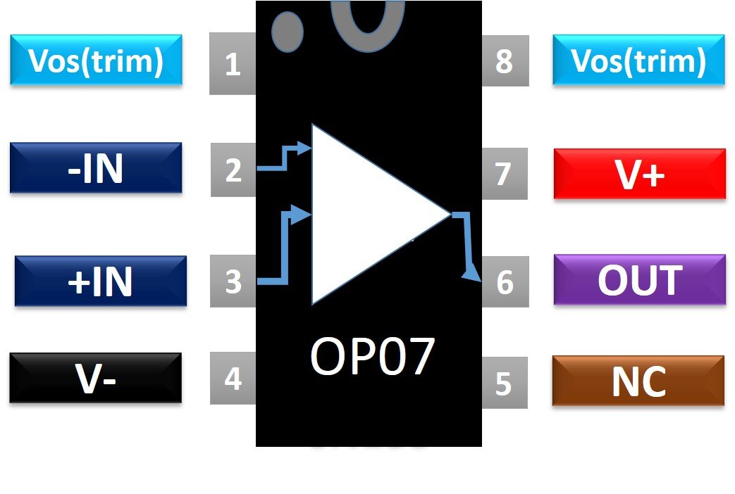
OP07 Pinout Diagram

Pin Configuration Description
- Pins2 and 3 are the positive and negative inputs of the amplifier whereas pin6 is the output.
- Pins1 and 8 are
TRIM. These two pins are used to set the offset voltage.
- Pins4 and 7 are power supply pin. Connect these pins to terminals of power supply.
- Pin5 is NC which means Not Connected.
Features
- The input offset voltage is very low. The maximum input offset voltage for OP07E is 75µV.
- The range for input voltage is ±14 V
- The range for supply voltage is from ±3 V to ±18 V.
- CMRR is high. For OP07E, it is of 106 dB.
- It has high input impedance and provides a low-noise operation.
Where to use it?
The OP07 IC has very low input bias current and high open loop gain but it does not affect the gain accuracy and maintains the accuracy along with linearity. These features make the OP07 IC useful for instrumentation applications which requires high gain. It provides highly accurate output even in non-inverting circuits due to high impedance at input.
How to use OP07?
To operate the OP07 chip, power on IC by supplying the voltage supply. It can operate using a single supply or dual supply which depends on the application. It can withstand maximum voltage of ± 22V. Voltage supply greater than this value can damage the chip permanently. Ideally both the inputs of operational amplifier should provide zero output when grounded but, in reality the inverting and non-inverting inputs are at different potentials.
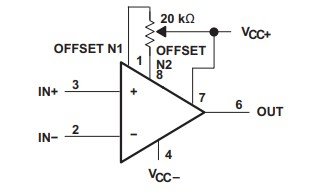
The reason for this might be mismatched collector currents, current gain, collector resistor, emitter resistor, etc. Therefore, the OP07 has two input offset pins to set the offset voltage through external circuitry in order to adjust these mismatches. Normally, we connect a resistor or a potentiometer between these input pins. By adjusting the resistance of a potentiometer, you can set the desired value. The potentiometer is mainly useful in applications that require precise offset control. The internal circuit of the OP07 amplifier limits the output voltage within ± 12 V. Figure 3 shows the circuit for setting input offset voltage.

OP07 Example Circuit
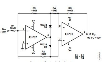
Figure below shows an absolute value circuit designed using two OP07 IC’s. It generates an output signal which follows the absolute value of input applied. The OA07 IC on left is working in inverting configuration. If the input voltage is positive, the output of the left OA07 IC will rise toward negative value.
The inverting input voltage will be greater than the non-inverting voltage. Diode D1 will pull back the inverting input down to zero. Therefore, the inverting input of the right OP07 chip will be -Ein. It is also working in inverting mode and its positive input is 0. Thus, the output of the right IC will be equal to Ein.

Now, lets see what happens when Ein goes negative. The inverting input of left IC will become virtual zero. In the equilibrium state, both inputs of the second OP07 IC will have voltage. The right OPO7 is operating in non-inverting mode so the output will be -Ein. In this case, Ein is negative therefore Eo will be positive value in a range of 0 to 10V.
Applications of OP07 Op Amp
The OP07 IC is useful in following applications:
- Wireless base station and optical networks
- Strain bridges
- Instrumentation
- Shunt current measurements
- Resistor thermal detectors (RTDs)
- Sensors and controls
- Thermocouples
- Precision filters
2D Diagram
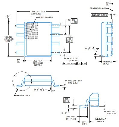
The 2D packages of OP07 include 8-lead PDIP and 8-lead SOIC. Figure given gives information regarding dimensions of SOIC package.

Check out Maxim op-amp part number MAX4238 / MAX4239 for an ultra low offset device.