This tutorial is about pinout and Features of LPC2148 Microcontroller. For developing different microprocessor based applications, the designer of embedded systems and SOC (system on chip) are used different processor cores, libraries, and tools. On these processors, libraries, and tools, the ARM7 is one of the best processors for embedded system designers. It has become so much popular in the last few years. It is easily available on the local market or online shops. This global ARM7 processor technology has developed so many microcontrollers such as LPC2144, LPC2146, and LPC2148, etc. But LPC2148 microcontroller is the most famous microcontroller which has been currently using in different applications such as in automatic braking systems and mobile phones etc. Here we will discuss the pin configuration with the features of LPC2148 microcontroller. Hopefully, this article will help out the reader to understating the features and pin configuration of LPC2148 microcontroller.
Recommended Components
The following parts are used in this article, along with a generic electronics kit that is handy for building and testing the circuit.
| Component | How it’s used | Buy on Amazon |
|---|---|---|
| LPC2148 ARM7 development board | An LPC2148 ARM7 board to work through the examples in this article. | Check Price |
| Electronic component assortment kit (1390 pcs) | A handy assortment of resistors, capacitors, LEDs, diodes and transistors for building circuits. | Check Price |
| Digital multimeter (AstroAI) | Measures voltage, current, resistance and checks continuity while you build and debug. | Check Price |
| Breadboard | Solderless base for prototyping the circuit. | Check Price |
| Jumper Wires | Make the connections on the breadboard. | Check Price |
As an Amazon Associate we earn from qualifying purchases. Prices and availability are accurate as of the date/time indicated and are subject to change.
Features of LPC2148 Microcontroller
LPC2148 microcontroller has developed by Philips (NPX semiconductor) company It has so many built-in peripherals and features. Therefore it has become so efficient and reliable as compared to other microcontrollers. It is 16 bit or 32 bit ARM 7 based microcontroller which as different features.
- It is 16 or 32 bit ARM 7 family-based microcontrollers and is available in market in small packages such as LQFP64.
- Its programming time is 1 millisecond for 256 bytes and 400 millisecond for erasing the on full chip data .
- It is used on-chip bootloader software during the ISP (in system programming) and IAP ( in application programming)
- It has 8 kB to 40 KB on chip static RAM and 32 kB to 512 kB on chip flash memory.
- It offers the high speed operation at frequency 60 MHz with wide range of interface almost 128 bit.
- LP218 has clock input with 32 K Hz frequency and low power RTC (real time clock).
- It has embedded ICE RT and embedded trace interface which offers the tracing of instruction execution with high speed with real time debugging.
- It offers a changeable output with 10 bit DAC( digital to analog converter).
- In this LQFP64 small package, it also has 5 volts input output pins for any general purposes.
- For counting the external events it has two 32 bit timers, watchdog timer and PWM unit.
- LPC2148 offers the changeable input with 10 bit ADC (analog to digital converter) with very conversion time such as 2.44μs / channel.
- The modes, which are used for power conversion are called idle and power down.
- It has several serial interfaces such as two 12C buses, two 16C550 UARTs with 400 Kbit speed.
- It has 1 MHz to 25 MHz on chip incorporated oscillator which works as an exterior crystal.
- It also has individual enable or disable peripheral function and peripheral SLK scaling for extra power optimization.
LPC2148 Microcontroller Pinout Diagram
LPC2148 microcontroller consists of 64 pins and the group of these pins is called a port. It consists of two ports and registers. These ports could be used as input or output ports therefore the pins of these ports are called GPIO (general purposes input-output ) pins. LPC 2148 microcontroller pin configuration figure is shown below,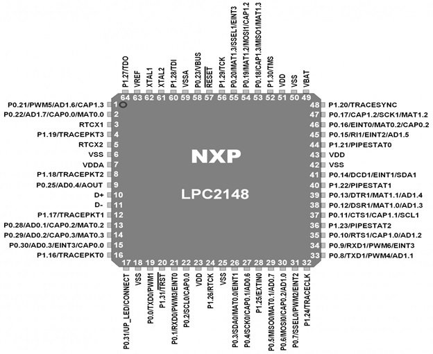
Figure 1 Pin Configuration of LPC 2148 Microcontroller
GPIO Pins Details
Pin1 (P0.21/PWM5/AD1.6/Cap1.3): It is a general-purpose pin and it could be used for four multiple ways such as it could be as input output data pin, as a pulse width modulation generator, as an analog to digital converter and as a capture input for timer l channel 3.
Pin 2 (P0.22/AD1.7/CAP0.0/MAT0.0): It could be for used for four purposes. First one P0.21, it could be used for input output data pin, second one AD1.7 , it could be used as analog to digital converter with ADC 1, input 7. Third one CAP0.0,it could be used as a capture input for timer 0 and channel 0. Fourth one MAT 0.0, it could be used as match output for timer 0 and channel 0.
Pin 3 (RTC X1): Pin3 is used as input pin for RTC oscillator circuit.
Pin 4 (P1.19/TRACEPKT3): Pin 4 could be as GPIO pin as well as with 3 bit input output pin for inner pull up.
Pin 5 (RTCX2): Pin 4 is used as output pin for RTC oscillator circuit.
Pin(6,18,25,42,50): These pins are used as references pins for grounding the microcontroller.
Pin7(VDDA): This pin is used as voltage source pin with 3.3 Volts. These voltages could be useful for on chip digital to analog converter and analog to digital converter.
Pin8(P1.18/TRACEPKT2): This pin is used as GPIO pin and 2 bit input output pin for inner pull up.
Pin9(P0.25/AD0.4/AOUT): This pin is used as GPIO pin, as input 4 for AD0 and as output pin for digital to analog converter.
Pin(10,11): Pin10 is used for D+ line bidirectional USB. Similarly the pin11 is used for D-line bidirectional USB.
Pin12(P1.7/TRACEPKT1): This pin is used as a GPIO pin and as a standard input/output port for inner pull up.
Pin13 (P0.28/AD0.1/CAP0.2/MAT0.2): This pin is used as a GPIO pin, analog to digital converter pin for ADC-0 input 1, capture input pin for timer 0 channel 2 and as a match output pin for timer 2 channel 1.
Pin14(P0.29/AD0.2/CAP0.3/MAT0.3): This pin could be used as a GPIO pin, converter input pin for ADC-0 input 2,capature input for timer 0 channel 3 and as a match output pin for timer 0 channel 3.
Pin15(P0.30/AD0.3/CAP0.3/EINT3/CAP0.0): This pin could be used as GPIO pin, converter pin for ADC-0 timer input 3,external interrupt with input 3 and as capture input pin for timer 0 channel 0.
Pin16(P1.16/ TRACEPKT0): This pin could be used as a trace packet pin as well as GPIO pin.
Pin(17,19,20,21): All these pins are used as GPIO pins. Pin17 is used as UP_LED pin, means it is used as indicator pin. Pin19 is used as a transmitter output for UART0 and as a pulse width modulator for output 1. Pin20 is used as a reset pin for JATG interface. Similarly the pin21is uses as receiver input for UART0,as PWM generator for output 3 and as external interrupt with input 0.
Pin(22,24,26,27,28,29,30): These are GPIO pins. Pin22 is used as clock input output and capture input pin, pin 24 is used as CLK output during JATG interface. Pin 26 is used as matched output for timer 0 channel 0 and as external interrupt for input1.Pin 27 is used as a serial clock for transferring data from master bus to slave bus and as a digital converter ADC-0.6 for input 6. Pin 28 could be used as external trigger input with inner pullup. Pin 29 is used as MISO for transferring data form mater to slave bus and used as a converter ADC-0 with input 7.Pin 30 is also used as MISO output and as a capture input for timer 0 channel 2.
Pin(23,43,51): These pins are used for suppling input voltages to internal core and input output ports.
Pin(31,32,33): These pins are used as GPIO pins. Pin 31 is used as SSEL0,PWM2 and as external interrupt for input 2.Pin 32 is used as a trace CLK for standard input output port with inner pull up. Similarly, pin 33 is used as transmitter TXD1 for UART1 and as a pulse width modulator PWM4
Pin(34,35,36,37): Pin 34,35,36 and 37 are GPIO pins. Pin 34 could be used as input receiver such as RDX1 for UART1, as output pulse modulator such as PWM6 for output 6.,as an external interrupt pin for input 3.Pin 35 could be used as a request pin for sending request to UART1 , as a capture input pin for timer 1 channel 1,as an anlage to digital converter ADC-1 for input 1.Pin 36 could be used as a 2-bit pipe line status pin for standard input output port. Pin 37 could be used as a clear input pin for UART1,as a capture pin for timer 1 channel and as a clear output input pin for 12C bus observer.
Pin(38,39,40,41): Pin 38,39,40 and 41 could be used as GPIO pin. Pin 38 could be used as an output data terminal ready pin for UART1,as match output pin for timer 1 channel 0 and as an analog to digital converter ADC-1 for input1.Pin 39 could be used as an input data terminal ready pin for UART1, as an output match pin for terminal 1 channel 1 and as a converter ADC-1 for input 4.Pin 40 could be used a bit-1 pipe line status pin for standard input output port. Pin 41 could be used as input data carrier detector pin for UART1,as an external interrupt pin for input 1 and as an input output open drain pin for 12C bus observer.
Pin(44,45,46,47): These pins are also used as GPIO pin. Pin 44 could be used as a bit-0 pipe line pin for standard input output port. Pin 45 could be used as an input ring pointer pin for UART1, as an external interrupt pin for input 2 and as a pulse width modulator generator ADC-1.5 for input 5.Pin 46 could be used as external interrupt pin for input 0, as a match output pin for timer 0 channel 2 and as a capture input pin for timer 0 channel 2. Pin 47 could be used as capture input pin for timer 1 channel 2,as a serial CLK pin for sending output from master but to slave bus.
So, the remaining pins of this LPC 2148 microcontroller are work same as explained pins.