6N135 is a single channel high speed optocoupler based on two photodiodes and a transistor output. It works by providing an electrical insulation shield between an input side and an output side. Compare to conventional optoisolators such as 4N24, MOC2031, 6N135 offers a very high speed bits transmission rate due to separate biasing voltages photodiode and transistor base-collector terminals.
A separate biasing voltage is provided to the base terminal of the transistor through a photodiode. Separate biasing voltage for the base terminal reduces the capacitance between the base-collector terminal. Hence, it helps to increase operating speed to a hundred times as compared to conventional optoisolators. Another equivalent of this optocoupler is 6N136. It can be used to provide electrical isolation between two circuits through an optical signal between an input side and an output side. The maximum operating frequency signal is up to 2MHz.
6N135 Pinout diagram
The pin diagram of an optocoupler is shown here. It has 8 pins but two pins are unused. Details and functions of all pins are listed in the next section.
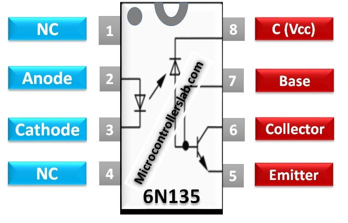
Pin Configuration details 6N135
| Pin Number | Pin Name | Function |
|---|---|---|
| 1 | NC | This pin is not used – No Connection |
| 2 | Anode (A) | Anode terminal of Infrared photodiode – Connect with logical high input |
| 3 | Cathode(C) | Cathode terminal of IR diode – Usually connect with the ground |
| 4 | NC | This pin is not used – No Connection |
| 5 | Emitter (Ground) | Emitter terminal of transistor – Connect with Ground terminal of output side circuit |
| 6 | Collector (Vo) | Collector terminal of transistor- Connect Isolated load through this pin |
| 7 | Base (VB) | Base terminal of transistor – Pull up resistor through Vcc pin and by default logic high signal |
| 8 | VCC | Connect 5 volts with this pin. |
Other optocouplers are:
How and Where to use?
As mentioned earlier, both 6N135 and 6N136 are exactly the same except the CTR (%) difference. Other electrical characteristics and the Pinout diagram are the same. Therefore, an example we discuss in this section works for both.
- This is a sample circuit diagram to use these optoisolators
- Vin signal of 1MHz frequency connects with anode pin through 330Ω current limiting resistor and another terminal ( cathode pin) connects with the ground
- At the output side, the Emitter pin connects with the ground to follow common emitter configuration
- Pull up resistor of 2.2k connects with the collector terminal
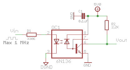
When you will connect the Vin signal with a 1MHz signal, you will get an inverted signal at the Vout pin. Because by default, 5 volts logic appears on the Vout terminal and when the transistor turns on, the ground signal appears on the Vout pin. In short, you will get an inverted output on the Vout pin as compared to the input signal.
Features 6N135 and 6N136
Some of the best features of 6N135 and 6N136 are listed below:
- It can withstand isolated voltage up to 5300 Vrms volts.
- External biasing voltage for transistor speeds up the operating speed up to 2MHz
- 6N135 supports a bandwidth of 2MHz
- The switching signal between the input and the output side can be as high as 1Mbits/sec.
- It is compatible with CMOS and TTL circuits. It’s mean either input or output sides can be either TTL or CMOS or both can be TTL/CMOS based.
- It is available in SMD-8 and DIP-8 packages.
Note: More information on Features and Specification are available in the datasheet.
Applications 6N135
We have listed the most important applications 6N135 optocoupler below:
- High-speed electrical signals isolations
- High voltage isolation circuits
- Video transmission circuit always require high bandwidth signal transfer between the control device and high voltage device
- Motor driver applications to isolate controller circuit from high power motor drive circuit
- High voltage Line signal conditioning
- Switch-mode power supplies for feedback of high voltage to the PID controller
- Ground isolation between TTL and CMOS devices
- It can be used to replace expensive pulse transformers
- Digital and Analog ground signal isolation.
Electrical Specifications of 6N136/6N135

- Maximum reverse voltage 5 volts and forward current 25mA for input photodiode
- IR Photodiode maximum power dissipation 45mW
- Supply voltage: 15 volts
- Output voltage: 15 volts
- Emitter base voltage through Vcc pin: 5 volts
- The maximum and normal output currents are 8mA and 16mA respectively.
- Output Power dissipation = 100mW
For more details on electrical specification check 6N135/6N136 DataSheet.
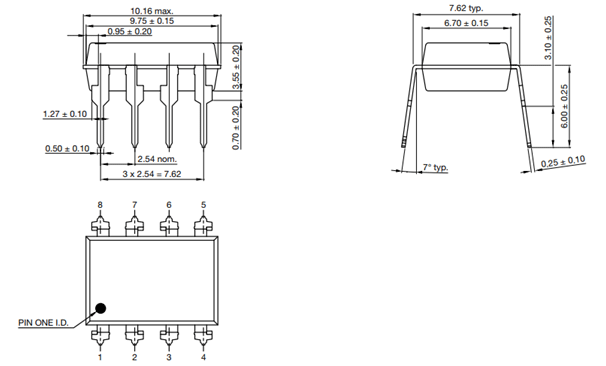
Physical Dimensions
This 2D diagram shows the physical dimension of the DIP-8 package. All dimensions are listed on a millimeter scale. For a 2D diagram of SMD IC, download datasheet from the link provided in the above section.
Can you tell me what purpose the Vb pin serves ? Only on your website did I find some information. Is Vb useful for something ? Looking thought internet and even the manufacturer supply no circuit example of it usefulness.
Regards,
Donald W.