In this tutorial, we will talk about 74LS83 4-bit full adder IC. Firstly, we will see an introduction of half and full adder. After that, we will learn to implement 4-bit full adder functionality using 74LS83.
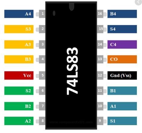
74LS83 Pin Configuration
The following figure shows the physical appearance of the IC is shown below. It is a 16 pin IC and available in multiple packages.

The pinout diagram of 74LS83 IC is given below:
Pinout Details
Now let’s discuss the functionality of each pin one by one.
- This IC has a total of 16 pins.
- Pin# 5 and 12 are used to power up IC with +5V and GND terminal of power supply respectively.
- Let say we have two 4 bit numbers as A4 A3 A2 A1 and B4 B3 B2 B1 with A1 and B1 as Least Significant Bit (LSB) of respective numbers. A4 and B4 as Most Significant Bit (MSB) of the same numbers.
- Pin#1,3,8,10 are input pins and will be used to feed A4 A3 A2 A1 bit of 1st number
- Pin#16,4,7,11 are input pins and will be used to B4 B3 B2 B1 bit of 2nd number.
- Pin#13 is an input pin and used to feed carry in.
- Pin#15,2,6,9 are output pins and will be used to observe the addition of two above numbers as S4 S3 S2 S1.
- Pin# 14 is an output pin and displays the resultant carry of addition.
Internal Logic Diagram
The logic diagram implemented inside 74LS83 using gates is given below for more clarity.

The truth table for this IC is given below:

4-Bit Full Adder Working
In order to understand 74LS83 full adder working, first, we need to understand half and full adder circuits. Now let’s explore these circuits one by one.
we will explore the following things.
- Adder
- Full Adder
- 4 Bit full Adder
- 4 Bit Full Adder using IC 74LS83
Half Adder
A digital circuit used to carry out the addition of numbers is called an adder in the electrical/electronic field. In the electronics/digital field usually, numbers are expressed in a binary format where 0 represents a logic low and 1 represents a logic high. To carry out complex tasks in the digital world often these simple 0s and 1s are processed using arithmetic operations i.e. addition, subtraction, multiplication, and division. In this topic; we are considering the addition of binary numbers and the circuitry used to perform this task is known as an adder.
Let’s consider two binary numbers consisting of a single bit. The simplest form of addition is shown in the table below.

A circuit that can carry out this simple task to give resultant sum and carry as output can be built using simple gates as shown below:

The above circuit performs the logic given in pic 1 and it is known as a half adder. As it can process only 2 single-bit numbers. Another logic circuit that can process 3 single-bit numbers is known as a full adder.
Full Adder
In full adder, 3 single bit number can be processed. There is a total of three inputs in this type of adder. Two inputs are our numbers to be added and the third input is the carry bit. It has two outputs known as the sum and carry out. The logic table of the full adder is given below.

A circuit that can perform this task can be built using gates as follows.

The advantage of a full adder is that by cascading two or more full adders we can perform the addition of numbers consisting of multiple bits.
4-Bit Adder
A 4-bit adder is a logic circuit which can perform the addition of two 4 bit numbers. The logic table for the 4-bit adder is given below.

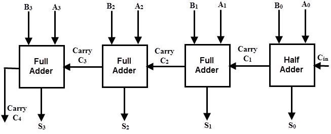
A circuit consisting of a combination of half and full single bit adder cascaded together to achieve desired results is shown below.
Full Adder using Logic Gates
Here it is worth elaborating that these half and full adders consist of simple transistors combined to perform these logic outputs already shown above. As the use of these concepts becomes familiar and the application of these gates expanded the manufacturers started developing integrated circuits in which they have already implemented these logics using transistors and we just can grab a single IC instead of using transistors individually to develop these gates.
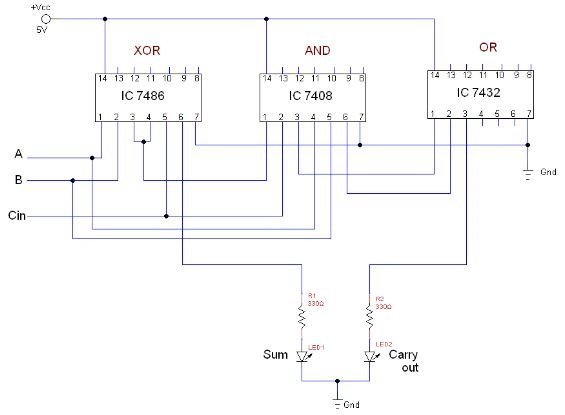
A few examples of these ICs are as follows.
- 74LS86 is an IC having XOR gates in it
- 74LS08 is an IC having AND gates in it
- 74LS32 is an IC having OR gates in it
So these IC can be used to implement full adder logic as shown below:
4-Bit Full Adder using 74LS83
On similar grounds, an IC has been developed which has already implemented 4-bit full adder logic in it. We just have to feed 4 bit 2 numbers at input and power supply. We don’t need to wire up the above circuit in pic 10 and it eases the task to implement a 4-bit full adder circuit.
Proteus Simulation
Let’s try to simulate this IC in proteus software and observe some of the input and output responses.
Suppose we have two numbers 1010 (10) as A4 A3 A2 A1and 1100 (12) as B4 B3 B2 B1 with carry C0 as 0. The resultant should be 10110 (22) as C4 S4 S3 S2 S1 and it can be observed in the pic below.
Suppose we have two numbers 1110 (14) as A4 A3 A2 A1and 1001 (9) as B4 B3 B2 B1 with carry C0 as 0. The resultant should be 10111 (23) as C4 S4 S3 S2 S1 and it can be observed in the pic below.

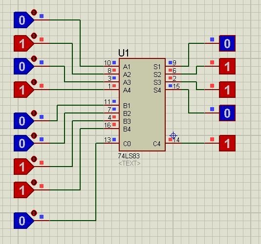
Suppose we have two numbers 1010 (10) as A4 A3 A2 A1and 1100 (12) as B4 B3 B2 B1 with carry C0 as 1. The resultant should be 10110 (22) as C4 S4 S3 S2 S1 and it can be observed in the pic below.

In this case
- A1=0, B1=1, C0=1 so A1+B1+C0=S1=0 and internal carry let’s say Ci=1.
- A2=1 B2=0, Ci (from previous step) =1 so A2+B2+Ci=S2=0 and internal carry let’s say Cii=1.
- A3=1 B3=0, Cii (from previous step) =1 so A3+B3+Cii=S3=0 and internal carry let’s say Ciii=1.
- A4=1 B4=1, Ciii (from previous step) =1 so A3+B3+Ciii=S3=1 and resultant carry C4=1.
Applications
- Arithmetic unit implementation
- Binary and Digital Counters
- Digital logic design projects
- Alarms and digital clocks
Alternative Full Adder ICs and Tutorials
- CD4560 NBCD Adder
- CD4008 4-Bit Full ADDER IC
- half adder and full adder simulation using PSpice
- Design half adder circuit in labview
- Design full adder circuit in labview
- Full Adder implementation using VHDL on basys 3 and 2 FPGA board
2D Diagram
The following picture shows the PDIP package of 74LS83 IC along with its dimensions.

A1=0, B1=1, C0=1 so A1+B1+C0=S1=0 and internal carry let’s say Ci=1.
Here you have taken B1=1 but in the above example you have taken this number 1100 (12) as B4 B3 B2 B1 where B1 = 0.