This STM32F4 Discovery Board ADC tutorial teaches you how to use the built-in Analog-to-Digital Converter of the STM32F407VG microcontroller using the HAL ADC driver in Keil uvision IDE. You will learn about the ADC peripheral architecture, all three ADC modules (ADC1, ADC2, ADC3), how analog input channels map to GPIO pins, how ADC resolution determines measurement precision, and how to write complete HAL-based code for both single-conversion (polling) and continuous-conversion modes. By the end, you will be able to read any analog voltage (from a potentiometer, sensor, or divider) connected to the STM32F4 Discovery Board and convert the raw ADC value into a real voltage in volts or millivolts.
The ADC is one of the most important peripherals on any microcontroller — every time you read a temperature from an LM35, a position from a joystick, a light level from an LDR, a battery voltage, or a current from an ACS712 sensor, you are using the ADC. This guide uses Keil uvision and the STM32CubeF4 HAL libraries, so the same code pattern transfers directly to any other STM32F4-based project you build later.
Recommended Components
The following components are used in this project or are helpful for getting started with STM32F4 Discovery board development.
| Component | How it’s used in this project | Buy on Amazon |
|---|---|---|
| STM32F4 Discovery Board | The STM32F407VG Discovery development board used in this project. | Check Price |
| Mini-USB Cable | Type-A to Mini-B cable to program and power the board over its onboard ST-Link. | Check Price |
| 10kΩ Potentiometer | Provides a variable 0–3.3 V analog input to test the ADC. | Check Price |
| Breadboard | Solderless board to mount the potentiometer and wiring. | Check Price |
| Jumper Wires | Connect the potentiometer to GND, PA0, and 3.3 V. | Check Price |
As an Amazon Associate we earn from qualifying purchases. Prices and availability are accurate as of the date/time indicated and are subject to change.
What You Will Learn
- The architecture of the STM32F407VG ADC: three 12-bit SAR ADC modules sharing 16 channels
- Which GPIO pins correspond to which ADC channels (AN0 through AN15)
- How ADC resolution (6/8/10/12-bit) affects the smallest measurable voltage
- How to calculate resolution and convert raw ADC values back into voltage
- The role of
ADC_HandleTypeDef,ADC_InitTypeDef, andADC_ChannelConfTypeDefin HAL configuration - How to configure the ADC clock, resolution, data alignment, and conversion mode
- A complete working example of single-conversion (polling) mode using ADC2 channel 0
- A complete working example of continuous-conversion mode using ADC1 channel 0
- How to wire a potentiometer to the STM32F4 Discovery Board for ADC testing
- How to view live ADC values in Keil’s debugger Watch Window
Prerequisites and Required Components
- STM32F4 Discovery Board (STM32F407G-DISC1)
- 10 kΩ potentiometer — provides a variable 0–3.3 V input for testing
- 3 jumper wires to connect the potentiometer to GND, PA0, and 3.3 V
- Mini USB cable for programming and power via the onboard ST-LINK/V2
- Keil uvision IDE with the STM32F4 device family pack installed
- Familiarity with the STM32F4 LED blinking tutorial and the push button tutorial — this tutorial assumes you can already create Keil projects and configure GPIO pins
STM32F4 Discovery Board ADC Modules
As mentioned in the introduction, the STM32F4 Discovery Board contains an ARM Cortex-M4 based STM32F407VG chip. This microcontroller has a rich set of built-in user-programmable peripherals, and ADC modules are one of the most important. The STM32F407VG provides three successive-approximation (SAR) type ADC modules: ADC1, ADC2, and ADC3. These three modules share 16 analog input channels, which means you have 16 multiplexed analog inputs available on the STM32F4 Discovery Board. Any of the three ADC modules can sample any of the shared channels — and because they are independent peripherals, you can run them simultaneously to achieve higher effective sample rates or to sample three different signals at once.
Having three independent ADCs is a big advantage over simpler microcontrollers like the Arduino Uno, which has only one 10-bit ADC. The STM32F4 can do 12-bit conversions at up to 2.4 Msps on each module, and they can be triggered by timers or synchronized for interleaved sampling.
STM32F4 ADC Pins and Channel Mapping
The STM32F407VG6T microcontroller ADC supports 6-bit, 8-bit, 10-bit, and 12-bit configurable resolution. It also supports three conversion modes: single, continuous, and scan (or discontinuous). The result of every A/D conversion is stored in a 16-bit data register, either left-aligned or right-aligned depending on your configuration.
The following table shows the GPIO pin that corresponds to each analog channel on each of the three ADC modules. Note that channels AN0–AN3 and AN10–AN13 share the same pin across all three ADCs (PA0–PA3, PC0–PC3), while some channels on ADC3 are routed to PORTF pins instead — which is why ADC3 behaves slightly differently on the Discovery Board where those PORTF pins are not easily accessible.
| Analog Channel | ADC1 | ADC2 | ADC3 |
|---|---|---|---|
| AN0 | PA0 | PA0 | PA0 |
| AN1 | PA1 | PA1 | PA1 |
| AN2 | PA2 | PA2 | PA2 |
| AN3 | PA3 | PA3 | PA3 |
| AN4 | PA4 | PA4 | PF6 |
| AN5 | PA5 | PA5 | PF7 |
| AN6 | PA6 | PA6 | PF8 |
| AN7 | PA7 | PA7 | PF9 |
| AN8 | PB0 | PB0 | PF10 |
| AN9 | PB1 | PB1 | PF3 |
| AN10 | PC0 | PC0 | PC0 |
| AN11 | PC1 | PC1 | PC1 |
| AN12 | PC2 | PC2 | PC2 |
| AN13 | PC3 | PC3 | PC3 |
| AN14 | PC4 | PC4 | PF4 |
| AN15 | PC5 | PC5 | PF5 |
STM32F407VG6T Microcontroller ADC Resolution
ADC resolution is defined as the smallest change in input voltage that the ADC can detect — in other words, how fine-grained your digital reading is. The maximum digital output value of an ADC depends directly on the number of bits: an 8-bit ADC outputs values from 0 to 255, a 10-bit ADC outputs 0 to 1023, and a 12-bit ADC outputs 0 to 4095 (the default on the STM32F4).
ADC resolution in volts per step can be calculated as:
Resolution = ( Operating voltage of ADC ) / 2^(number of bits ADC)
The operating (reference) voltage of the STM32F4 Discovery Board is 3.3 V. If we configure the ADC in 12-bit mode:
Resolution = 3.3V/2^12 = 3.3/4095 = 0.8mV
This means the ADC’s digital output will increment by 1 for every 0.8 mV change on the input pin. If you apply exactly 3.3 V to the analog input, the digital output will be 4095 (the maximum 12-bit value). If you apply 0 V, the digital output will be 0.
To convert a measured digital value back into a real voltage, multiply the digital value by the resolution. For example, if the ADC returned 3500:
Input Voltage = 3500 x 0.8mV = 2800mV or 2.8V
The STM32F4 ADC can be used in a wide range of applications: AC voltage measurement, AC current measurement, power measurement, battery monitoring, temperature sensing, audio input, joystick reading, and any other task that requires converting a real-world analog signal into a number your firmware can process.
STM32F4 HAL ADC Driver Overview
In this section we will walk through the CubeHAL ADC APIs used to configure and initialize ADC channels on STM32F4 series microcontrollers. HAL keeps the ADC configuration clean and portable: three C structures do most of the work — ADC_HandleTypeDef, ADC_InitTypeDef, and ADC_ChannelConfTypeDef.
ADC Handler Struct
The most important C struct is ADC_HandleTypeDef. This struct represents a single ADC module and is passed by pointer to every HAL ADC function call.
typedef struct
{
  ADC_TypeDef      *Instance;
  ADC_InitTypeDef   Init;
  __IO uint32_t         NbrOfCurrentConversionRank;
  DMA_HandleTypeDef         *DMA_Handle;
  HAL_LockTypeDef               Lock;
  __IO uint32_t                 State;
  __IO uint32_t                 ErrorCode;
}ADC_HandleTypeDef;
Let’s look at what each member does:
*Instance: Pointer to theADC_TypeDefregister block for the ADC module you want to use — eitherADC1,ADC2, orADC3.Init: An instance ofADC_InitTypeDefused to select clock prescaler, resolution, scan mode, data alignment, conversion mode, number of conversions, and so on.NbrOfCurrentConversionRank: The current conversion rank in a multi-channel sequence.*DMA_Handle: Pointer to a DMA handle. We will use this in a follow-up tutorial on ADC + DMA.
ADC Initialization Struct
ADC_InitTypeDef holds the configuration for a single ADC module:
typedef struct
{
  uint32_t ClockPrescaler;
  uint32_t Resolution;
  uint32_t DataAlign;
  uint32_t ScanConvMode;
  uint32_t EOCSelection;
  FunctionalState ContinuousConvMode;
  uint32_t NbrOfConversion;
  FunctionalState DiscontinuousConvMode;
  uint32_t NbrOfDiscConversion;
  uint32_t ExternalTrigConv;
  uint32_t ExternalTrigConvEdge;
  FunctionalState DMAContinuousRequests;
}ADC_InitTypeDef;
Configuring the ADC Clock
The ADC clock (ADCCLK) is common to all three ADC modules on the STM32F4. It is derived from the APB2 bus and can be divided further by a programmable prescaler: Fpclk/2, /4, /6, or /8. The ClockPrescaler field in ADC_InitTypeDef selects this divisor.
Since APB2 runs at up to 84 MHz on a fully-clocked STM32F4, using a /2 prescaler gives the ADC a 42 MHz clock, while /8 gives 10.5 MHz. Higher clocks mean faster conversions but can reduce accuracy on high-impedance sources. For beginners, /8 (the slowest option) is a safe default.
In the HAL ADC driver, the prescaler is set using one of the following macros:
#define ADC_CLOCK_SYNC_PCLK_DIV2    0x00000000U
#define ADC_CLOCK_SYNC_PCLK_DIV4    ((uint32_t)ADC_CCR_ADCPRE_0)
#define ADC_CLOCK_SYNC_PCLK_DIV6    ((uint32_t)ADC_CCR_ADCPRE_1)
#define ADC_CLOCK_SYNC_PCLK_DIV8    ((uint32_t)ADC_CCR_ADCPRE)
Setting the ADC Resolution
The Resolution member of ADC_InitTypeDef selects the ADC output width — 6, 8, 10, or 12 bits. Higher resolution means more precision but slower conversion time, because the SAR algorithm needs one clock cycle per resolution bit.
#define ADC_RESOLUTION_12B  0x00000000U
#define ADC_RESOLUTION_10B  ((uint32_t)ADC_CR1_RES_0)
#define ADC_RESOLUTION_8B   ((uint32_t)ADC_CR1_RES_1)
#define ADC_RESOLUTION_6B   ((uint32_t)ADC_CR1_RES)
- Scan Mode (
ScanConvMode): Enables/disables scan mode, which is used when you want to sample multiple channels in sequence with a single trigger.
Data Alignment (DataAlign)
DataAlign sets the format of the digital output — either right-justified (standard, value occupies the lower bits) or left-justified (value occupies the upper bits, useful for easy scaling to 16-bit). For beginners, always use right alignment.
#define ADC_DATAALIGN_RIGHT      0x00000000U
#define ADC_DATAALIGN_LEFT ((uint32_t)ADC_CR2_ALIGN)- Continuous Conversion Mode (
ContinuousConvMode): Selects whether the ADC performs a single conversion per trigger, or runs continuously forever.
The remaining fields (scan mode, number of conversions, DMA, external triggers) will be covered in follow-up tutorials on STM32F4 multi-channel ADC and ADC with DMA.
STM32F4 ADC Single-Channel, Single-Conversion Mode Example
Now let’s put everything together in a working example that measures an analog voltage using the STM32F4 Discovery Board’s ADC in single-channel, single-conversion mode. In this mode, each call to HAL_ADC_Start() triggers exactly one conversion on one channel — the simplest and most controllable setup, ideal for slow applications like temperature logging or battery monitoring.
For this example we will configure ADC2, channel 0 (AN0), which maps to pin PA0.
The first step is to enable the clock for the GPIO port of the analog input pin. AN0 is multiplexed with PA0, so we enable the clock to PORTA:
__HAL_RCC_GPIOA_CLK_ENABLE();The next step is to configure PA0 as an analog input pin using GPIO_InitTypeDef. The same struct we used in the LED blinking and push button tutorials is used here, except this time the mode is GPIO_MODE_ANALOG instead of output or input.
/* Configure and initialize PA0 pin as analog input pin for A/D conversion */
void Configure_GPIO(void)
{
	 __HAL_RCC_GPIOA_CLK_ENABLE(); // enable clock to GPIOA
	GPIO_InitTypeDef ADCpin; //create an instance of GPIO_InitTypeDef C struct
	ADCpin.Pin = GPIO_PIN_0; // Select pin PA0
	ADCpin.Mode = GPIO_MODE_ANALOG; // Select Analog Mode
	ADCpin.Pull = GPIO_NOPULL; // Disable internal pull-up or pull-down resistor
	HAL_GPIO_Init(GPIOA, &ADCpin); // initialize PA0 as analog input pin
}
HAL ADC Configuration
With PA0 configured as an analog input, we now configure the ADC peripheral itself. Before configuring anything, enable the clock to the ADC module using __HAL_RCC_ADCx_CLK_ENABLE(), where x is the ADC number. We are using ADC2:
__HAL_RCC_ADC2_CLK_ENABLE()Next, set parameters such as resolution, data alignment, end-of-conversion event, and clock prescaler using ADC_InitTypeDef fields, then call HAL_ADC_Init() to apply them.
Declare an instance of ADC_HandleTypeDef as a global variable — global because we will use the same instance across multiple HAL ADC function calls in main():
ADC_HandleTypeDef myADC2Handle;Select the ADC module by assigning its register base to the Instance field:
myADC2Handle.Instance = ADC2; // create an instance of ADC2Set the resolution to 12-bit via the Init.Resolution field:
myADC2Handle.Init.Resolution = ADC_RESOLUTION_12B; // select 12-bit resolution We are using ADC2 in single-channel, single-conversion mode. Setting EOCSelection to ADC_EOC_SINGLE_CONV tells the HAL that the end-of-conversion flag should fire after every single conversion:
myADC2Handle.Init.EOCSelection = ADC_EOC_SINGLE_CONV; //select single conversion as a end of conversion eventAlign the result right-justified so the raw 12-bit value sits in the lower bits of the 16-bit register:
myADC2Handle.Init.DataAlign = ADC_DATAALIGN_RIGHT; // set digital output data right justifiedFinally, pass a pointer to myADC2Handle into HAL_ADC_Init() to apply all of these settings to the ADC2 peripheral:
HAL_ADC_Init(&myADC2Handle); // initialize AD2 with myADC2Handle configuration settingsHAL Select ADC Channel
So far we have only configured the ADC2 module itself — we have not told it which channel to actually sample. HAL_ADC_ConfigChannel() selects and configures the channel:
HAL_StatusTypeDef HAL_ADC_ConfigChannel(ADC_HandleTypeDef* hadc, ADC_ChannelConfTypeDef* sConfig)The first argument is the ADC_HandleTypeDef we already configured. The second is an ADC_ChannelConfTypeDef struct that describes which channel, what rank (position in a multi-channel sequence), sampling time, and offset.
Here we create an ADC_ChannelConfTypeDef named Channel_AN0, select channel 0, set it to rank 1 (first and only channel in the sequence), and choose a 15-cycle sampling time. Longer sampling times are needed for high-impedance sources (like a potentiometer) to let the internal sample-and-hold capacitor settle.
ADC_ChannelConfTypeDef Channel_AN0; // create an instance of ADC_ChannelConfTypeDef
Channel_AN0.Channel = ADC_CHANNEL_0; // select analog channel 0
Channel_AN0.Rank = 1; // set rank to 1
Channel_AN0.SamplingTime = ADC_SAMPLETIME_15CYCLES; // set sampling time to 15 clock cycles
HAL_ADC_ConfigChannel(&myADC2Handle, &Channel_AN0); // select channel_0 for ADC2 module.
Read the ADC Digital Output
Inside your main loop, where you want to take a reading, start the conversion with HAL_ADC_Start(), passing a pointer to your ADC_HandleTypeDef:
HAL_ADC_Start(&myADC2Handle);Then wait for the conversion to finish by polling HAL_ADC_PollForConversion(). The first argument is the ADC handle; the second is a timeout in milliseconds.
HAL_StatusTypeDef HAL_ADC_PollForConversion(ADC_HandleTypeDef* hadc, uint32_t Timeout);This function returns a HAL_StatusTypeDef enum value. When the conversion succeeds, it returns HAL_OK.
typedef enum
{
  HAL_OK       = 0x00U,
  HAL_ERROR    = 0x01U,
  HAL_BUSY     = 0x02U,
  HAL_TIMEOUT  = 0x03U
} HAL_StatusTypeDef;
We wrap the poll in an if statement with a 5 ms timeout:
if(HAL_ADC_PollForConversion(&myADC2Handle, 5) == HAL_OK)Read the converted value with HAL_ADC_GetValue() and store it in a uint32_t variable:
Adc_value = HAL_ADC_GetValue(&myADC2Handle); // read digital value and save it inside uint32_t variableFinally, stop the ADC until the next reading:
HAL_ADC_Stop(&myADC2Handle); // stop conversion Complete STM32F4 ADC Single-Conversion Code
#include "stm32f4xx_hal.h"

void Configure_GPIO(void);
void configure_ADC2_Channel_0(void);
void Delay_ms(volatile int time_ms);

uint32_t Adc_value;
ADC_HandleTypeDef myADC2Handle;
int main(void)
{
	Configure_GPIO(); // initialize PA0 pin
	configure_ADC2_Channel_0(); // configure ADC2
	while(1)
	{
	 HAL_ADC_Start(&myADC2Handle); // start A/D conversion
		if(HAL_ADC_PollForConversion(&myADC2Handle, 5) == HAL_OK) //check if conversion is completed
		{
		Adc_value  = HAL_ADC_GetValue(&myADC2Handle); // read digital value and save it inside uint32_t variable
		}
		HAL_ADC_Stop(&myADC2Handle); // stop conversion
		Delay_ms(200);
	}
}

/* Configure and initialize PA0 pin as analog input pin for A/D conversion */
void Configure_GPIO(void)
{
	 __HAL_RCC_GPIOA_CLK_ENABLE(); // enable clock to GPIOA
	GPIO_InitTypeDef ADCpin; //create an instance of GPIO_InitTypeDef C struct
	ADCpin.Pin = GPIO_PIN_0; // Select pin PA0
	ADCpin.Mode = GPIO_MODE_ANALOG; // Select Analog Mode
	ADCpin.Pull = GPIO_NOPULL; // Disable internal pull-up or pull-down resistor
	HAL_GPIO_Init(GPIOA, &ADCpin); // initialize PA0 as analog input pin
}
void configure_ADC2_Channel_0(void)
{
__HAL_RCC_ADC2_CLK_ENABLE(); // enable clock to ADC2 module
	myADC2Handle.Instance = ADC2; // create an instance of ADC2
	myADC2Handle.Init.Resolution = ADC_RESOLUTION_12B; // select 12-bit resolution
	myADC2Handle.Init.EOCSelection = ADC_EOC_SINGLE_CONV; //select  single conversion as a end of conversion event
	myADC2Handle.Init.DataAlign = ADC_DATAALIGN_RIGHT; // set digital output data right justified
	myADC2Handle.Init.ClockPrescaler =ADC_CLOCK_SYNC_PCLK_DIV8;
	HAL_ADC_Init(&myADC2Handle); // initialize AD2 with myADC2Handle configuration settings

  /*select ADC2 channel */
	ADC_ChannelConfTypeDef Channel_AN0; // create an instance of ADC_ChannelConfTypeDef
	Channel_AN0.Channel = ADC_CHANNEL_0; // select analog channel 0
	Channel_AN0.Rank = 1; // set rank to 1
	Channel_AN0.SamplingTime = ADC_SAMPLETIME_15CYCLES; // set sampling time to 15 clock cycles
	HAL_ADC_ConfigChannel(&myADC2Handle, &Channel_AN0); // select channel_0 for ADC2 module.
}
void Delay_ms(volatile int time_ms)
{
	      int j;
        for(j = 0; j < time_ms*4000; j++)
            {}  /* excute NOP for 1ms */
}
Potentiometer Wiring for STM32F4 ADC Test
To test the code, connect a 10 kΩ potentiometer to the STM32F4 Discovery Board as shown below. As you turn the knob, the voltage at PA0 sweeps smoothly between 0 V and 3.3 V, which lets you verify the full range of ADC values from 0 to 4095.

| Potentiometer | STM32F4 Discovery Board |
|---|---|
| Right Pin | GND |
| Center Pin | PA0 |
| Left Pin | 3.3V |
If this is your first Keil project, follow our getting-started guides before building this ADC code:
- LED Blinking Tutorial STM32F4 Discovery Board
- Use Push Button to Control LEDs of STM32F4 Discovery Board
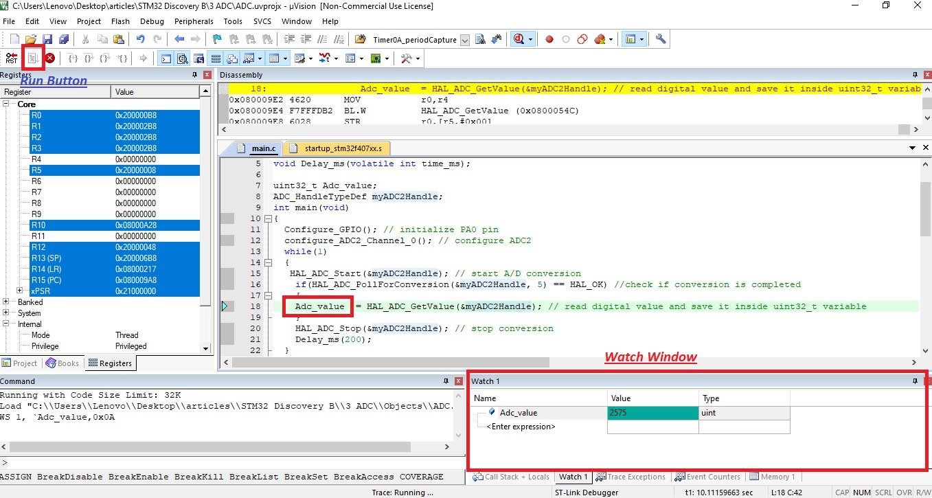
Viewing the ADC Values in the Keil Debugger
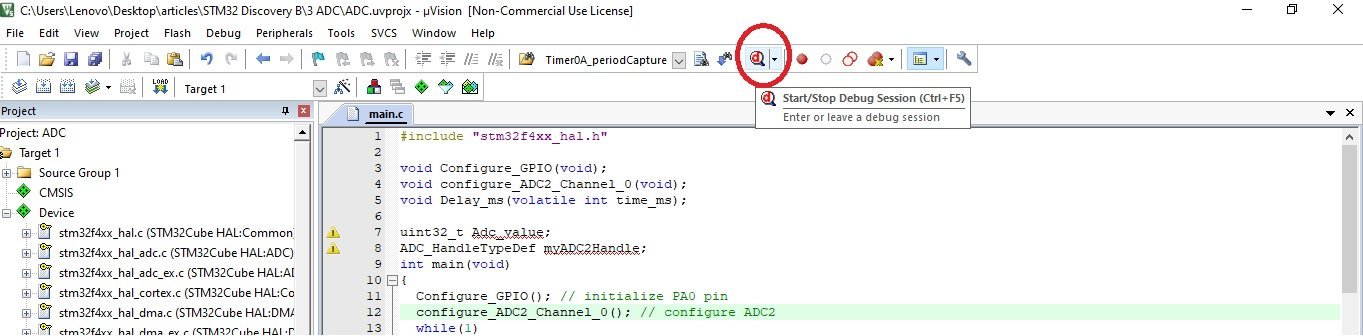
To watch the digital output of the ADC live, compile and build the project (F7), then start a Keil debugging session by clicking the debugger icon:
In the debugging window, add the Adc_value variable to the Watch Window (View → Watch Windows → Watch 1), then press F5 to run. As you rotate the potentiometer, the value in the Watch Window will update between 0 (at 0 V) and 4095 (at 3.3 V), confirming that ADC2 channel 0 is sampling PA0 correctly.
STM32F4 ADC — Convert Digital Value into Voltage
The raw ADC value (0–4095) is rarely what you actually want — you usually want the voltage in volts or millivolts, especially when working with sensors. Converting is easy: multiply the raw value by the resolution. At 12-bit mode with Vref = 3.3 V, the resolution is 0.8 mV/step, so the voltage in volts is:
voltage = (Adc_value * 3.3) / 4095;
The code below reads PA0 and calculates the equivalent voltage in real time. Integer arithmetic is used to avoid floating-point overhead — the result is in volts with the decimal fixed via the /10000 divisor.
double voltage;
int main(void)
{
	Configure_GPIO(); // initialize PA0 pin
	configure_ADC2_Channel_0(); // configure ADC2
	while(1)
	{
	 HAL_ADC_Start(&myADC2Handle); // start A/D conversion
		if(HAL_ADC_PollForConversion(&myADC2Handle, 5) == HAL_OK) //check if conversion is completed
		{
		Adc_value  = HAL_ADC_GetValue(&myADC2Handle); // read digital value and save it inside uint32_t variable
		voltage = (Adc_value * 8 ) / 10000;
		}
		HAL_ADC_Stop(&myADC2Handle); // stop conversion
		Delay_ms(200);
	}
}
In upcoming tutorials we will cover STM32F4 ADC with DMA (for high-throughput sampling without CPU intervention), ADC with interrupts (for event-driven sampling), and ADC triggered by hardware timers (for precise sampling intervals needed in signal processing).
STM32F4 ADC in Continuous Conversion Mode
The single-conversion mode we just covered is fine for slow applications that need 1–2 samples per second, but many real applications need fast, continuous sampling — think audio, vibration monitoring, or closed-loop control. For these, use continuous conversion mode.
Continuous mode can be used with a single channel or with multiple channels. This tutorial focuses on single-channel continuous mode. In continuous mode, the ADC performs A/D conversions back-to-back on its own — as soon as one conversion finishes, the next one starts, without any CPU involvement. You do not need to call HAL_ADC_Start() repeatedly in the main loop; just start once and read the latest value whenever you need it.
STM32F4 Continuous Conversion Mode Code
#include "stm32f4xx_hal.h"
void Configure_GPIO(void);
void configure_ADC1_Channel_0(void);
void Delay_ms(volatile int time_ms);

ADC_HandleTypeDef myADC2Handle;
 uint32_t rawValue;
 float temp;
int main(void)
{
   Configure_GPIO(); // initialize PA0 pin
	configure_ADC1_Channel_0(); // configure ADC2
	while(1)
	{

 //HAL_ADC_PollForConversion(&myADC2Handle, HAL_MAX_DELAY);

 rawValue = HAL_ADC_GetValue(&myADC2Handle);
 temp = ((float)rawValue) / 4095 * 3300;
	}
}

/* Configure and initialize PA0 pin as analog input pin for A/D conversion */
void Configure_GPIO(void)
{
	 __HAL_RCC_GPIOA_CLK_ENABLE(); // enable clock to GPIOA
	GPIO_InitTypeDef ADCpin; //create an instance of GPIO_InitTypeDef C struct
	ADCpin.Pin = GPIO_PIN_0; // Select pin PA0
	ADCpin.Mode = GPIO_MODE_ANALOG; // Select Analog Mode
	ADCpin.Pull = GPIO_NOPULL; // Disable internal pull-up or pull-down resistor
	HAL_GPIO_Init(GPIOA, &ADCpin); // initialize PA0 as analog input pin
}
void configure_ADC1_Channel_0(void)
{
__HAL_RCC_ADC1_CLK_ENABLE(); // enable clock to ADC1 module
	myADC2Handle.Instance = ADC1; // create an instance of ADC2
	myADC2Handle.Init.ClockPrescaler =ADC_CLOCK_SYNC_PCLK_DIV8;
	myADC2Handle.Init.Resolution = ADC_RESOLUTION_12B; // select 12-bit resolution
	myADC2Handle.Init.ScanConvMode = DISABLE;
	myADC2Handle.Init.ContinuousConvMode = ENABLE;
	myADC2Handle.Init.DiscontinuousConvMode = DISABLE;
	myADC2Handle.Init.DataAlign = ADC_DATAALIGN_RIGHT; // set digital output data right justified
        myADC2Handle.Init.NbrOfConversion = 1;
        myADC2Handle.Init.DMAContinuousRequests = DISABLE;
        myADC2Handle.Init.EOCSelection = ADC_EOC_SEQ_CONV;

	HAL_ADC_Init(&myADC2Handle); // initialize AD2 with myADC2Handle configuration settings

  /*select ADC2 channel */
	ADC_ChannelConfTypeDef Channel_AN0; // create an instance of ADC_ChannelConfTypeDef
	Channel_AN0.Channel = ADC_CHANNEL_0; // select analog channel 0
	Channel_AN0.Rank = 1; // set rank to 1
	Channel_AN0.SamplingTime = ADC_SAMPLETIME_480CYCLES; // set sampling time to 15 clock cycles
	HAL_ADC_ConfigChannel(&myADC2Handle, &Channel_AN0); // select channel_0 for ADC2 module.
}
void Delay_ms(volatile int time_ms)
{
	      int j;
        for(j = 0; j < time_ms*4000; j++)
            {}  /* excute NOP for 1ms */
}
Troubleshooting STM32F4 ADC Issues
- ADC value stuck at 0 or 4095. The pin is not configured as
GPIO_MODE_ANALOG, or the pin is physically floating (no source connected). Verify wiring and check that you enabled the GPIOA clock. - ADC value always reads 4095. The input voltage exceeds 3.3 V — this saturates the ADC and risks damaging the pin. Always scale your input to stay within 0 V to Vref.
- Random / noisy ADC readings. The sampling time is too short for your source impedance. Increase
SamplingTimetoADC_SAMPLETIME_84CYCLESorADC_SAMPLETIME_480CYCLES. Also add a 100 nF decoupling cap close to the analog pin and keep the signal wire short. - HAL_ADC_PollForConversion returns HAL_TIMEOUT. The ADC clock is not enabled, or the ADC is stuck in a bad state. Double-check
__HAL_RCC_ADC2_CLK_ENABLE()and increase the poll timeout. - ADC value does not change when the potentiometer rotates. You wired the potentiometer incorrectly — the wiper (center pin) must go to PA0, with the outer pins going to 3.3 V and GND.
- Values look fine but voltage conversion is wrong. Remember Vref on the Discovery Board is 3.3 V, not 5 V. Using 5 V in your math will give the wrong result.
Frequently Asked Questions
How many ADCs does the STM32F4 Discovery Board have?
The STM32F407VGT6 on the STM32F4 Discovery Board has three independent 12-bit SAR ADC modules (ADC1, ADC2, ADC3) that share 16 analog input channels. The three ADCs can run simultaneously, so you can sample three different signals at once or interleave them for higher effective sample rates.
What is the maximum ADC resolution on the STM32F4?
12-bit — 4096 discrete output steps. Lower resolutions of 10-bit, 8-bit, and 6-bit are also available via the Resolution field and give faster conversion times at the cost of precision.
What is the reference voltage (Vref) of the STM32F4 ADC?
On the STM32F4 Discovery Board, Vref+ is tied to the 3.3 V supply rail, so the ADC’s full-scale input range is 0 V to 3.3 V. Any voltage above 3.3 V will either saturate the ADC or damage the pin — use a voltage divider or op-amp buffer for larger signals.
What is the difference between single and continuous ADC conversion mode?
In single-conversion mode, each HAL_ADC_Start() call produces exactly one sample — good for slow, on-demand readings. In continuous-conversion mode, the ADC samples back-to-back on its own; the CPU can read the latest value at any time without re-triggering. Continuous mode is best for fast signals, audio, and control-loop applications.
How do I convert the ADC raw value to voltage?
Multiply the raw ADC value by the resolution (Vref / 2^bits). For a 12-bit ADC at Vref = 3.3 V, that’s voltage = (raw_value * 3.3) / 4095. For integer-only math, scale both sides: voltage_mV = (raw_value * 3300) / 4095.
Why do I need a long sampling time for high-impedance sensors?
The ADC uses an internal sample-and-hold capacitor that must charge up to the input voltage before conversion. High source impedance (potentiometers above 50 kΩ, some temperature sensors) takes longer to charge this capacitor. Increase SamplingTime to ADC_SAMPLETIME_144CYCLES or ADC_SAMPLETIME_480CYCLES to give the capacitor more time, or add a low-output-impedance buffer op-amp between the sensor and the ADC pin.
Conclusion
This STM32F4 ADC tutorial took you from the ADC architecture of the STM32F407VG all the way to a working HAL-based program that samples an analog voltage from PA0 and converts the raw value back into a real voltage. You have now used the third fundamental GPIO mode — analog input — to complement the digital output and digital input you learned in the previous two tutorials. Coming up next we will look at the DAC peripheral, which does the reverse: it lets the STM32F4 Discovery Board generate analog waveforms on its own pins.
Thanks Sir,
The Video is very helpful to learn the ADC of STM32F4XX.
Thanks once again
hello, in your continuous conversion main, you didn’t start the ADC:
HAL_ADC_Start(&myADC2Handle);
or am i missing something?
Yes you need to start the ADC outside the while loop in main otherwise it won’t work.
how many ohms for the potentiometer ?