The CD4027 IC is a dual J-K Master/Slave flip-flop IC. This IC contains two JK flip flops having complementary outputs such as Q and ~Q. Each JK flip flop has control and input pins such as reset, set, clock and JK inputs. It belongs to the CD4000 series of integrated circuits constructed with N- and P-channel enhancement mode transistors. All inputs of CD4027 are protected against static discharge by diodes which are clamped to VDD and VSS. It is available in a variety of 14-pin packages which includes PDIP, GDIP, PDSO.
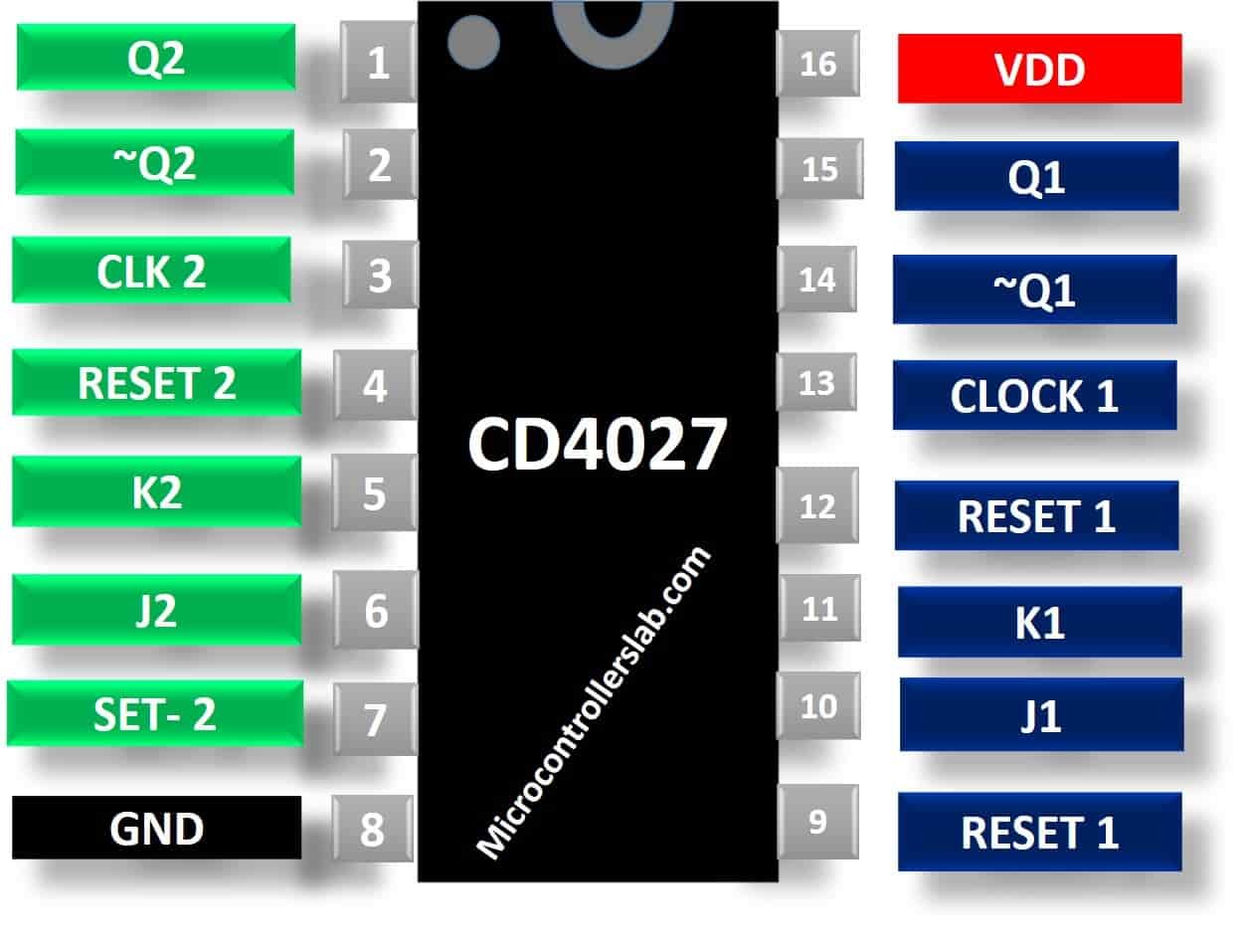
CD4027 JK Flip Flop Pinout Diagram
CD4027 dual JK flip-flop comes with 16 pins. The picture depicts a pinout diagram.
Pin Configuration Description
This CD4027 IC has a total of 16 pins. As it is a dual flip flop IC, so it has 2 flip flops. All the pins, their name, and description are mentioned in the table given below.
| Pin Number | Pin Name | Description |
|---|---|---|
| 1, 15 | Q2, Q1 | Output pins |
| 2, 14 | , | Inverted Output pins |
| 3, 13 | CLOCK 2, CLOCK 1 | Clock pulse |
| 4, 12 | RESET 2, RESET 1 | When this pin is LOW, the value of Q will be 1.
When this pin is HIGH, the value of inverted output () will be 1. |
| 5, 11 | K2, K1 | Input Pin 1 |
| 6, 10 | J2, J1 | Input pin 2 |
| 7, 9 | SET 2, SET 1 | When this pin is HIGH, the value of Q will be 1.
When this pin is LOW, the value of inverted output () will be high. |
| 8 | Negative power Supply | |
| 16 | Positive power supply |
CD4027 Features
- CD4027 Dual JK Flip Flop Package IC which operates at medium speed of 16 MHz typically with 10V supply
- Voltage range of 3.0V to 15V
- Static Flip-Flop Operation
- High noise immunity of 0.45 VDD(typ.)
- Set and Reset capability
- TTL compatible
- Low power of 50 nW (typ.)
- Input Rise/Fall time at 5V: 45us
- Maximum and minimum Input Voltage is 2 V and 0.8 V
Note: You can always refer to a datasheet for more features and Electrical specifications. The link of the datasheet is given at the end of the tutorial.
Alternative Options
74LS73, 74LS76, CD4013B, CD4042, CD4043, CD4095
Where to use it?
This CD4027IC is used for storing data and in performing control, register, and toggle functions. In toggling applications, it is used to alter the signal by control inputs. You can also use this IC in latching devices due to its property of storing data and determining the output based on the previous output.
How to use CD4027?
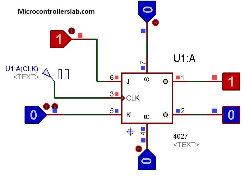
CD4027 has two flip flops each having independent four inputs and two outputs that work opposite to each other. The input pins J and K control the state of flip flop which occurs at the positive transition of clock pulse. We can provide a clock signal through a push button or a PWM signal. Set and reset pins are independent of the clock. They are initiated by applying a High signal on these pins. Pin 8 is connected to the ground. Connect pin 16 with power supply and switch on the supply.
This is a simple circuit diagram along with all control and clock signals. As you can see, reset and set signals are set to zero. Therefore, outputs on Q and ~Q pins are according to JK inputs. You can see the truth table to find a relation between input and output pins.
JK Flip Flop Truth Table
The truth table shown below describes the effect of applying different values at inputs on the outputs and next state of cd4027 flipflop.
| PRESENT STATE | NEXT STATE | ||||||
|---|---|---|---|---|---|---|---|
| CLOCK | J | K
| SET | RESET | Q | Q | |
| Positive edge | 1 | X | 0 | 0 | 0 | 1 | 0 |
| Positive edge | X | 0 | 0 | 0 | 1 | 1 | 0 |
| Positive edge | 0 | X | 0 | 0 | 0 | 0 | 1 |
| Positive edge | X | 1 | 0 | 0 | 1 | 0 | 1 |
| Negative edge | X | X | 0 | 0 | X | No Change | No Change |
| X | X | X | 1 | 0 | X | 1 | 0 |
| X | X | X | 0 | 1 | X | 0 | 1 |
| X | X | X | 1 | 1 | X | 1 | 1 |
Now let’s design a practical example with CD4027 JK flip flop IC.
4 bit Counter using CD4027 JK Flip Flop
In this example, we will design a synchronous counter using four FF. In synchronous counter offers no propagation delay. Because we connect clock signals with the clock pin of every FF. Consequently, all JK FF changes their state immediately on every positive edge. This 4-bit counter example consists of 4 JK flip flops, two AND gates CD4081 and one BCD based seven segment display. Although, this is a 4-bit counter and we can display decimal number from 0-16. But for demonstration purposes, we use only one seven-segment display.
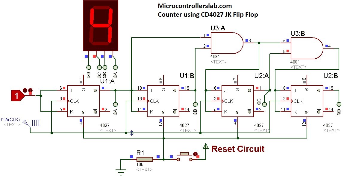
Counter Proteus simulation
As you can see from this proteus simulation, we give a common clock signal to all flip-flips. In other words, all FF make the transition of digital logic with the same clock signal. We connect the JK pins together. Because we want to transfer a logic high signal to each FF on a positive edge of the clock.
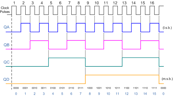
Each FF changes state according to this timing diagram.
CD4027 Applications
This IC has numerous applications. Some of them are:
- Computer memory circuits
- Shift Registers can be constructed using this IC as they are sequential logic circuits mainly used for storage of digital data
- Employed in voice registers and Memory or Control Registers due to is latching property
- EEPROM circuits for holding a small amount of data
- Latching devices and Counters
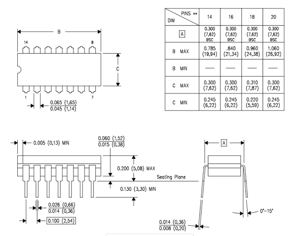
Two-dimensional Diagram
Datasheet
Related Electronics Components:
- CD4026 5-stage Johnson decade Counter Examples
- INTRODUCTION TO PIC18F4550 MICROCONTROLLER
- INTRODUCTION TO FIELD PROGRAMMABLE GATE ARRAYS (FPGA)
- CD4022 Divided by 8 Counter IC
- D Flip Flop design simulation and analysis using different software’s
- In-Depth 555 timer IC complete guide
- CD4042 Quad D Latch IC
- CD4017 Counter IC Examples
- CD4015 4-Stage Shift Register Serial in/Parallel Out
- 74HC157 Quad 2×1 Multiplexer IC
- In Depth Guide: NE556 Dual Timer IC(O