In this tutorial, we will explain the workings of a simple digital system known as a D flip flops. At the start, we will provide a brief and concise introduction to flip flops. After this, we will provide an explanation of the output they will show. A flip flop is another form of latch that can store memory in two or more states. After that, we will simulate the circuit using PSPICE and compare the result with the theoretical discussion (which should be the same). At the end of the tutorial, we have provided an exercise for you to do on your own, and in the next tutorials, we will assume that you have done those exercises and not explain the concept regarding them.
Introduction to D Flip Flop
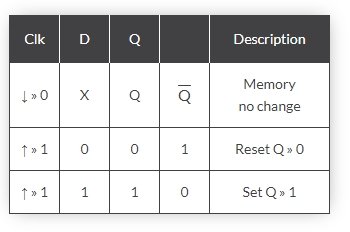
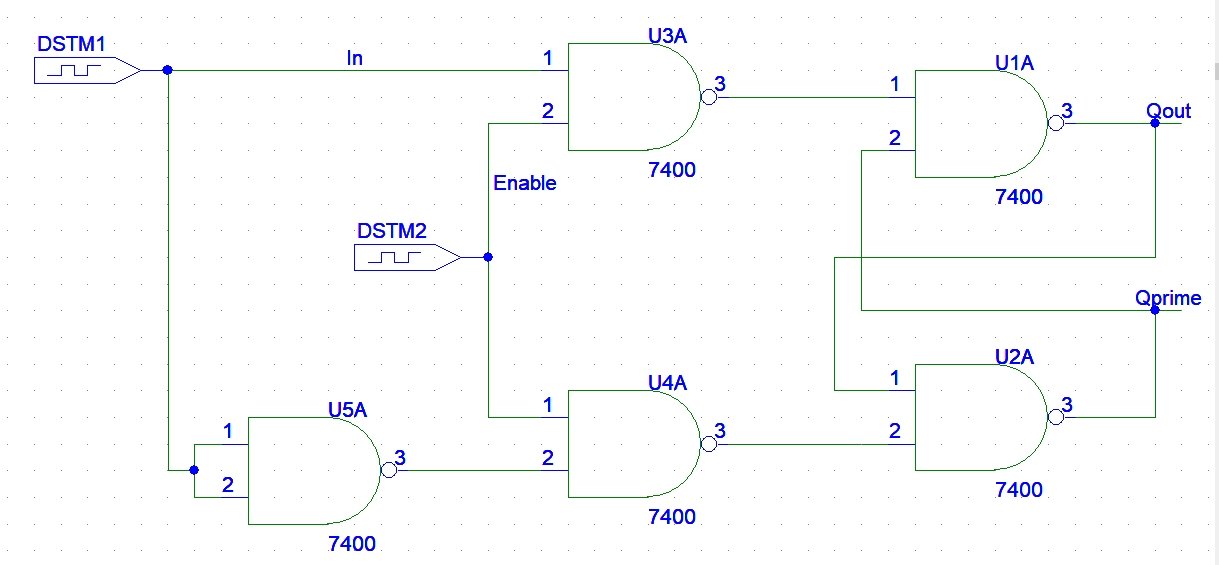
A D flip flop, also known as a Master-Slave flip flop. It is a modified form of a set-reset (SR) flip flop. Only the reset side of the flip flop is passes through an inverter, as shown in the figure below.

The Q output of the D or Data flip flop will be the same as the input if the enable is 1, and Q will show the previous input if the enable is 0. However, the Q’ output is the inverted form of Q, as shown in the truth table below.
Simulation of D Flip Flop in PSpice
Let’s design a simple digital circuit for a flip flop. We will not use built-in blocks; instead, we will use NAND gates, or we can also use the combination of AND and NOT gates, as we will explain shortly in this tutorial. Open the PSpice design manager on the PC by typing design manager in the search bar. From the design manager, click on the run schematic button to open a new blank schematic, as shown in the figure below.

After opening the new schematic, before jumping into designing, first save the schematic by clicking on the file button at the top left corner and then selecting save as so that we can access it anytime in the future. Refer to the figure below.

Click on the Get New Part icon at the top bar of the schematic window in order to search for the components that are needed for circuit design.

Placing Components
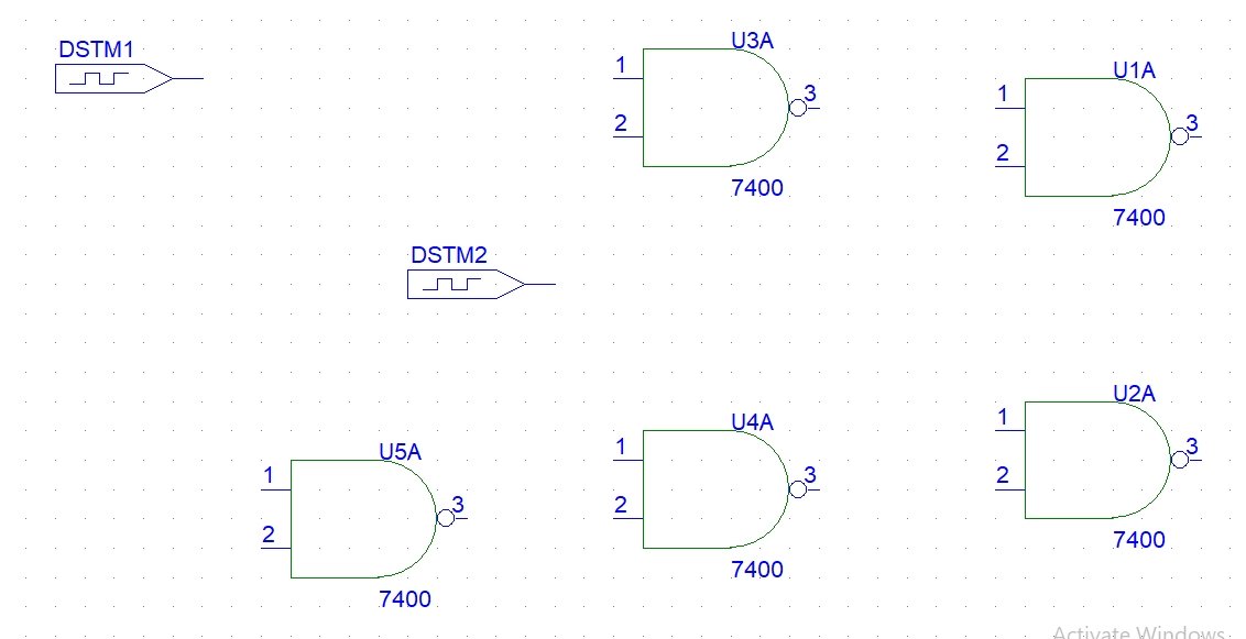
In the Get New Part window, type 7400. It will display a NAND gate available in PSPICE. From that list, select a simple NAND gate, as shown in the figure below.

If we want to build the circuit shown in the introduction, type ‘7408’ to place an AND gate. Again, open the Get New Part window, and in the part name block type STM, select the digital supply from the list given, and then click on Place & Close as shown in the figure below.

The components placed in the schematic window are shown in the figure below.
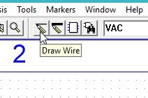
Click on the draw wire icon at the top bar of the schematic window in order to connect the already placed components for circuit design, as shown in the figure below.
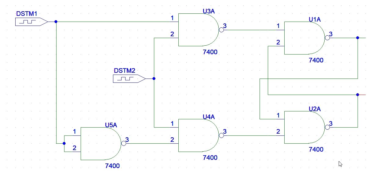
Complete Circuit Diagram
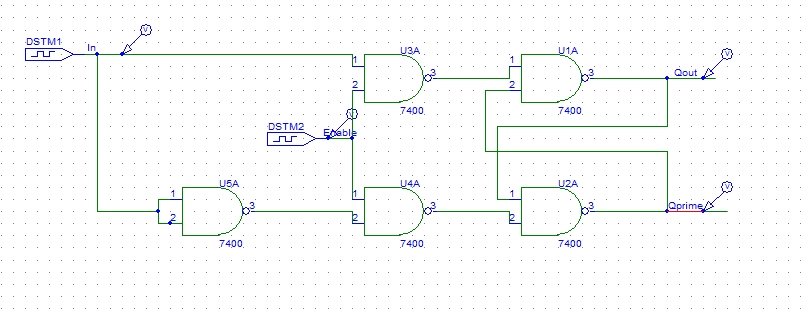
Connect all the components to complete the circuit diagram as shown in the figure below.
If we are interested in checking the voltage on a specific wire in spite of checking it at a node, double-click on the wire, and in the window that appears as a result, we will type the name of the wire to label it with, as shown in the figure below.

The labeled diagram of the D flip flop is shown in the figure below.
Voltage Marker
We can also change the name of the device, i.e., in this case, we have 2 identical sources, but each of these has a separate purpose. One of the sources is used as an input for the flip flop, and the other is used to enable the flip flop. If we want to display the voltage at a specific node of the circuit diagram, we can do this by placing a voltage marker at that node. On the top of the schematic window, click on the Voltage/Level Marker button, as shown in the figure below.

Place it at the output and at the input nodes. Also place a voltage marker at the enable of the flip flop, as shown in the figure below.
Input Attributes
The next step is to set the attributes of the input digital supply. Double-click on the dstm1 supply you connected in the circuit previously and set the input commands of the digital input system as shown in the figure below.

The commands in the attributes window represent the value of the input at the corresponding time in the command before the space. The COMMAND1 = 0s 0 shows that at time 0s the value of the input dstm is 0, and the COMMAND2 = 1s 1 shows that the value will update to 1 at time 1 second. Similar is the case with COMMAND5 = 4s 0, where at 4 seconds the value of the input will be 0.
The next step is to set the attributes of the input digital supply. Double-click on the dstm2, which is used as the enable source of the flip flop supply you connected in the circuit previously, and set the input commands of the digital input system, but these commands may or may not be the same as the commands of input 1, as shown in the figure below.

Simulation Setup
After this, we will adjust the properties of the simulations in order to produce a graph of the voltage at the marker. Click on analysis and then click on Setup, as shown in the figure below.

A window will appear. Click on the transient block on the window and adjust the properties of the window according to your requirements. Refer to the figure below.

Simulation
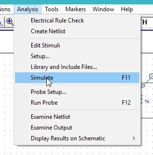
The final time of the response is 4 ms because we have set the commands for only up to 4 ms. Now comes the simulation part. Click on the analysis at the top bar of the schematic window and then click on simulate, as shown in the figure below.
A schematic window will appear showing the voltage at the output wire and the input source, as shown in the figure below.
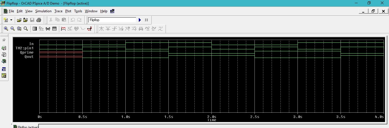
The output of the schematic is in accordance with the output discussed in the introduction part. The enable will control the output of the flip flop. When the enable is one, the Q output of the flip flop will give the input as it is, and the Q’ output will give the inverted input. When the enable is zero, the Q output will give the previous input value at the output, and the Q’ output will give the previous inverted input at the output. At the start, the red line at the outputs shows that there was no previous input, i.e., the input was not assigned any value in the previous state. As the enable is zero at the start, the output will be the previous input state, which is undefined.
Exercise
- Design a JK flip flop using the criteria discussed in this tutorial.
Conclusion
In conclusion, this tutorial provides an in-depth overview of designing and simulating D flip flops in PSpice. It covers step-by-step procedure with explanation of example to help us better understand the concept of D flip flops. You can utilize this concept to build more complex applications. At the last, an exercise reinforces the concept of D flip flops. Hopefully, this tutorial was helpful in expanding your knowledge in regards to designing and simulating using PSpice software.
You may also like to read:
- ESP32 Send Emails Through SMTP Server (Plain text, HTML, and Attachments)
- BME680 with ESP32 using Arduino IDE (Gas, Pressure, Temperature, Humidity)
- Telegram Control ESP32 and ESP8266 GPIOs and LEDs using Arduino IDE
- Serial Communication 8051 Microcontroller using KEIL
- AT89S52 8-bit Microcontroller with 8K Bytes In-System Programmable Flash
- 74HC595 Shift Register Interfacing with Arduino
This concludes today’s article. If you face any issues or difficulties, let us know in the comment section below.