In this tutorial, we will explain the workings of a simple digital system known as an adder. As the name implies, an adder adds two or more digital numbers. At the start, we will provide a brief and concise introduction to adders, specifically the simplest half adder. Then we will provide an example with an explanation and the output it will show. After that, we will simulate the circuits using PSpice and compare the result with the theoretical discussion (which should be the same). At the end of the tutorial, we have provided an exercise for you to do on your own, and in the next tutorials, we will assume that you have done those exercises and not explain the concept regarding them.
Introduction to Half Adder and Full Adder Circuits
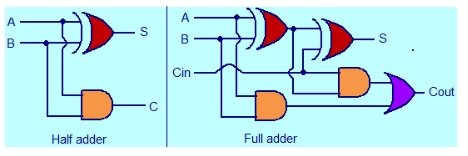
An adder is a digital circuit that provides the addition of two or more numbers. A half adder is used to perform the addition between two numbers, and if we are willing to add three numbers (digital) together, then we will use a full adder. A circuit diagram of a half adder and a full adder is shown in the figure below.
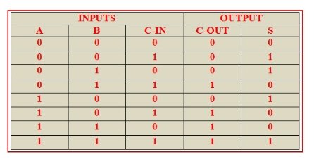
We should also take a glance at the truth tables of these adders. The truth table of the half-adder will have two inputs, as shown in the truth table given below:

Below is the truth table of a full adder, which you can use to complete the exercise given at the end.
Half Adder Simulation using PSpice
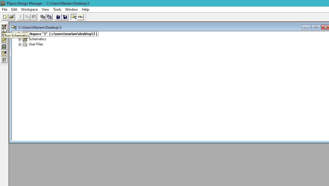
Let’s design a simple digital circuit for an adder. Here we will design the half adder and leave the full adder as an exercise for the reader. To design a half adder, we will use XOR and AND gates. Open the PSpice design manager on the PC by typing design manager in the search bar. From the design manager, click on the run schematic button to open a new blank schematic, as shown in the figure below.
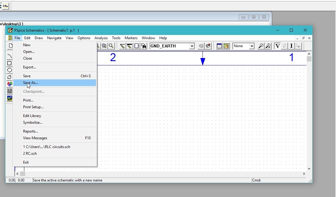
After opening the new schematic, before jumping into designing, first save the schematic by clicking on the file button at the top left corner and then selecting save as so that we can access it anytime in the future. Refer to the figure below.
Click on the Get New Part icon at the top bar of the schematic window in order to search for the components that are needed for circuit design.

Placing Components
In the Get New Part window, type 7486. It will display an XOR gate available in PSPICE. From that list, select a simple XOR gate, as shown in the figure below.

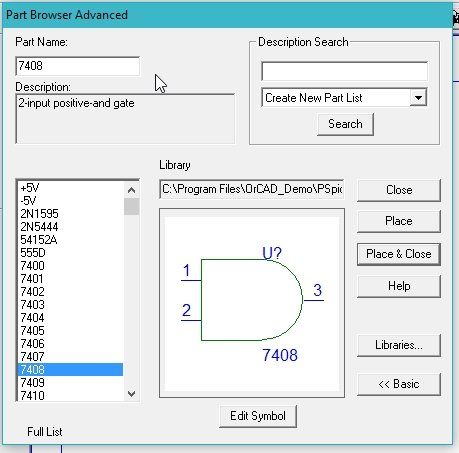
Again, open the Get New Part window, and in the part name block, type 7408. Select the AND gate from the list given and then click on Place & Close, as shown in the figure below.
Again, open the Get New Part window, and in the part name block, type STM. Select the digital supply from the list given and then click on Place & Close, as shown in the figure below.

The components placed in the schematic window are shown in the figure below.

Click on the draw wire icon at the top bar of the schematic window in order to connect the already placed components for circuit design, as shown in the figure below.

Complete Circuit Diagram
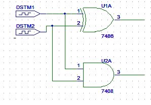
Connect all the components to complete the circuit diagram, as shown in the figure below.
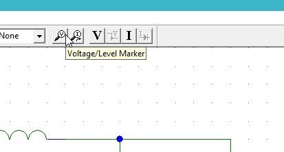
If we want to display the voltage at a specific node of the circuit diagram, we can do this by placing a voltage marker at that node. On the top of the schematic window, click on the Voltage/Level Marker button, as shown in the figure below.
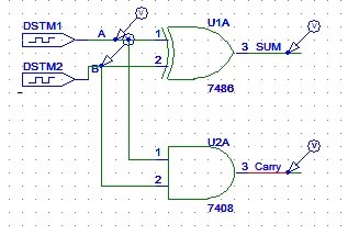
Place it at the output, i.e., the sum and the carry nodes, and at the input A and B nodes, also place a voltage marker as shown in the figure below.

If we are interested in checking the voltage on a specific wire in spite of checking it at a node, double click on the wire, and in the window that appears as a result, we will type the name of the wire to label it with, as shown in the figure below.

The labeled diagram of the half adder is shown in the figure below.
Input Attributes
The next step is to set the attributes of the input digital supply. Double-click on the dstm1 supply we connected in the circuit previously and set the input commands of the digital input system as shown in the figure below.
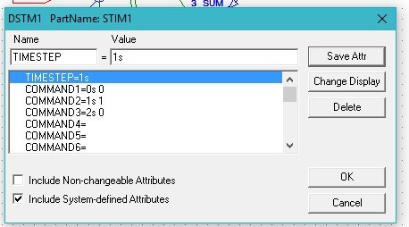
The commands in the attributes window represent the value of the input at the corresponding time in the command before the space. The COMMAND1 = 0s 0 shows that at time 0s the value of the input dstm is 0, and the COMMAND2 = 1s 1 shows that the value will update to 1 at time 1 second. Similar is the case with COMMAND3 = 2s 0, where at 2 seconds the value of the input will be 0.
The next step is to set the attributes of the input digital supply. Double-click on the dstm2, which is used as the supply source B we connected in the circuit previously, and set the input commands of the digital input system as shown in the figure below.

Simulation Setup
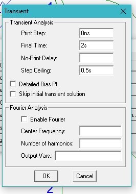
The next step is to adjust the properties of the simulations in order to produce a graph of the voltage at the marker. Click on analysis and then click on Setup, as shown in the figure below.

A window will appear. Click on the transient block on the window and adjust the properties of the window according to the requirements. Refer to the figure below.
Simulation
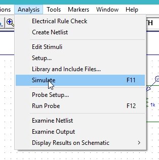
The final time of the response is 2s because we have set the commands for only 2s. Now comes the simulation part. Click on the analysis at the top bar of the schematic window and then click on simulate, as shown in the figure below.
A schematic window will appear showing the voltage at the output wire and the input source, as shown in the figure below.
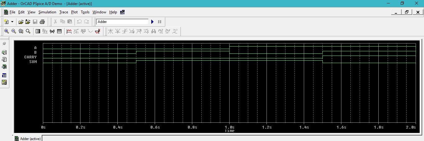
The output of the half adder is in accordance with the theoretical analysis, as we can see from the figure above.
Exercise
- Design and Simulate the full adder using the information provided in the introduction part and the procedure in the explanation portion
Conclusion
In conclusion, this tutorial provides an in-depth overview of designing and simulating a half adder circuit in PSpice. It covers step-by-step procedures along with examples and explanations, which helps us better understand the concept of an adder circuit. You can utilize this concept to build a full adder circuit or more complex circuits. At last, an example reinforces the concept of designing an adder circuit. Hopefully, this tutorial was helpful in expanding your knowledge of PSpice.
You may also like to read:
- BME680 Web Server with ESP32 ( Arduino IDE)
- Heart beat pulse sensor interfacing with pic microcontroller
- HC-05 Bluetooth Module with STM32 Blue Pill using STM32CubeIDE
- BeagleBone Black Pinout, Pin Configuration and Features
- Difference between RISC and CISC
- Serial Communication 8051 Microcontroller using KEIL
This concludes today’s article. If you face any issues or difficulties, let us know in the comment section below.