In this tutorial, we will explain the working of a simple digital system known as a digital encoder. At the start, we will provide a brief and concise introduction to encoders, specifically the simplest 4×2 encoder, with an explanation of the output they will show. An encoder is the opposite of a decoder or a multiplexer. It is used to encode numbers into binary digits, as we will see shortly. After that, the circuit will be simulated using PSPICE, and the results will be compared with the theoretical discussion provided (which should be the same). You are provided with an exercise to do it by yourself at the end of the tutorial. In the next tutorials, we will assume that you have done those exercises, and we will not explain the concepts regarding them.
Digital Encoder Introduction

An encoder, in its simplest terms, is a circuit, device, software program, or person that can convert information from one format or type to another. In the digital world, however, encoders are devices that can change binary digits from one format to another. The block diagram of a simple 4×2 encoder is shown in the figure below:
Figure 1: Block diagram of encoder


This encoder will encode a four-bit binary number into a two-bit binary number. The internal diagram of a simple 4×2 encoder is shown in the figure below.
Figure 2: Encoder circuit diagram

Figure 3: Truth table of encoder
If the value of A0 is 1, then the output will represent a binary 0. If A1 is 1 and all others are zero, then the output will be a binary 1. The truth table of a 4×2 encoder is shown in the figure below.
This implies that when A0 is 1 the output will represent 0 (00) and when A3 is 1 the output will show 3 (11) as is obvious from the above truth table.
Digital Encoder Simulation using PSpice
An encoder in its simplest form is a 4×2 encoder. By 4×2, we mean that the number of inputs is 4 (the first term of the name) and the number of outputs is 2. An encoder, as we have discussed above, is used to encode digital numbers from one format to another. Let’s now design the circuit for an encoder on PSPICE using the techniques we used previously. Write design manager in the search bar of your laptop. PSPICE Design Manager will open. After that, click on the run schematic button to open the schematic, as shown in the figure below:

Figure 4: Opening new schematic
After opening the schematic, before designing the circuit on the schematic, it is important to save it so that you can use it in the future. Click on the file icon at the top and then click on “Save As” or simply press Ctrl+S on the keyboard to save the schematic, as shown in the figure below:
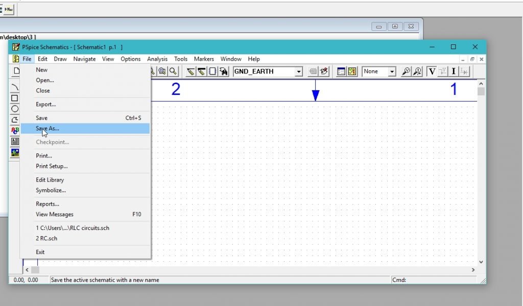
Figure 5: Saving schematic
At the top bar of the schematic, you simply need to click on “Get New Part”. This block contains all the components that may be needed for simulating an electric circuit, as we have done in previous tutorials. Please refer to the figure below to see the “Get New Part” option.

Figure 6: Getting a new part
In the search portion of the “get new part” block, type ‘7432’. This will show you an OR gate. As is obvious from the circuit given in the introductory part, an OR gate is the main component of the encoder. Please refer to the figure below:
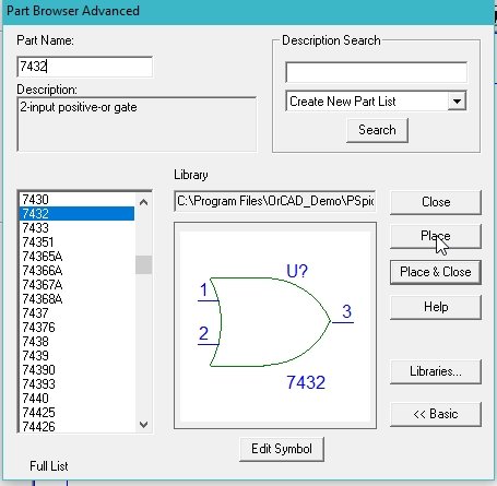
Figure 7: Placing OR gate
Again, open the get new part block and in the part name, type stm. This will show a list of digital sources. Select a simple digital source and place it next to the OR gates. Refer to the figure below:
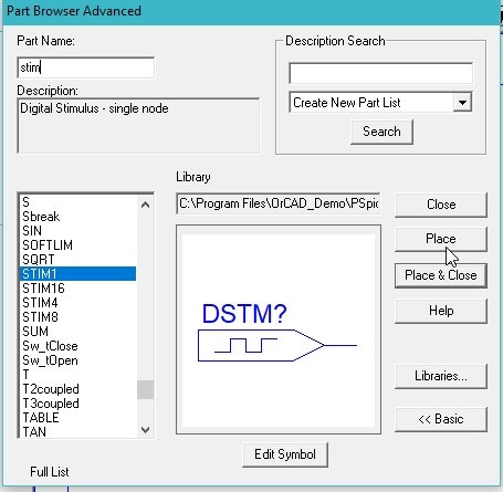
Figure 8: Placing digital source
The components required for an encoder circuit are shown in the figure below:
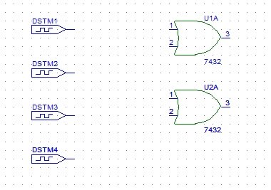
Figure 9: Placed components
Now, in order to complete the circuit diagram, we need to connect the components. To connect them, we use the draw wire block, as shown in the figure below:

Figure 10: Drawing wire
After connecting all the connections, the complete circuit thus formed is shown in the figure below:
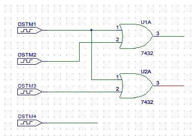
Figure 11: Complete circuit diagram
The digital source at the bottom of the circuit diagram represents the input source A0. As you can see from the figure of the circuit diagram in the introduction part, A0 is not connected to any component as shown in the circuit diagram above. The next step is to place the voltage marker at the input and output nodes of the circuit. A voltage marker is placed at the node where we want to examine the voltage. From the top of the schematic, select the voltage marker as shown in the figure below:
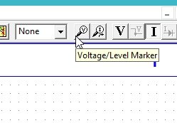
Figure 12: Voltage marker
Place the voltage marker at the output ends of the OR gate and at each end of the input digital source. The placed voltage markers are shown in the figure below:

Figure 13: Voltage marker
If we are interested in viewing the voltage waveform at a specific line or wire, we can also label it. Double-click on the line you want to label and give it a suitable name, as shown in the figure below:

Figure 14: Labeling a line
After labeling all the input and output wires, the circuit diagram will look like the one shown in the figure below:

Figure 15: Labeled circuit diagram
We can also name any device according to its use in the circuit. Double-click on the device you want to label and in the “Package reference designator” block, type the name you want to give to the device. Naming a device is done only to differentiate it from other sources, and there is no other purpose to naming a device. Refer to the figure below to understand how to label a device:

Figure 16: Labeling a device
After labeling all the devices according to their use in the circuit, the circuit will look like the one shown in the figure below:

Figure 17: Labeled devices.
Next step is to adjust the attributes of the input devices. As there is no use for the A0 digital source in the circuit diagram and it is only placed for understanding purposes, we can also remove it. The functionality will remain the same, and we will adjust the attributes of all the signals according to the truth table given in the introduction part.

Figure 18: Attributes of A0
A0 will be 1 at the end of the 4s simulation, as it is obvious from the truth table.
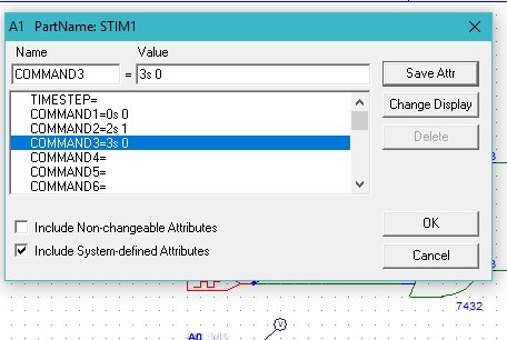
Figure 19: Attributes of A1
A1 will be 1 for 1s before the previous source i.e. A0 was 1, and zero otherwise, as shown in the figure above. Before A1, A2 was one, i.e., 1 for 1s, as shown in the figure below.
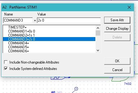
Figure 20: Attributes of A2
And at the very start, A3 will be one, and zero otherwise, as shown in the figure below:
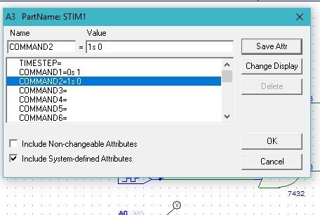
Figure 21: Attributes of A3
For simulation setup, click on the analysis tab at the top and then select “setup” as shown in the figure below:

Figure 22: Simulation setup
After that, click on the transient block and adjust the properties of the transient as shown in the figure below:

Figure 23: Transient block
The next step is to simulate the circuit you have designed. Click on the analysis button once again and then click on simulation, as shown in the figure below:

Figure 24: Simulation
Another window will pop up, displaying the output of the circuit you designed, as shown in the figure below:
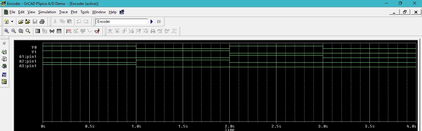
Figure 25: Output of the encoder
If we compare the output of the encoder with the truth table they both will be same.
Exercise
- Design an 8×3 encoder using the same techniques provided in this tutorial.
Conclusion
In conclusion, this tutorial provided an in-depth understanding of digital encoders, specifically focusing on the simple 4×2 encoder. The tutorial explained the working principle of an encoder, its block diagram and internal circuitry, and the truth table for encoding binary numbers. The tutorial also demonstrated how to simulate the encoder circuit using PSPICE, step-by-step. By following the instructions, users were able to design and simulate the encoder circuit, and compare the results with the theoretical discussion. Finally, the tutorial concluded with an exercise to further practice and enhance the knowledge gained. With the knowledge acquired from this tutorial, users can now move on to designing more complex encoders and exploring further applications of digital systems.
You may also like to read:
- Tracking Type ADC -Up/Down Counter Analog to Digital Converter
- Counter Type ADC – Staircase Approximation Analog to Digital Converter
- Single Slope and Dual Slope ADC – Integrating Analog to Digital Converter
- Flash ADC: Explained with 3-bit Flash Analog to Digital Converter Example Circuit
- Successive Approximation ADC – Analog to Digital Converter
- R-2R Ladder DAC – Explained with Example Circuit Diagram
- Binary Weighted Resistor DAC