In this tutorial, we will explain the workings of digital systems. We can use them for information processing in digital form, i.e., while working with computers. At the start, we provide a brief and concise introduction to digital systems, specifically the exclusive OR and exclusive NOR gates, along with their circuit diagrams and an explanation of the output they will show. After that, we simulate the circuits using PSPICE and compare the results with the theoretical discussion (which should be the same). At the end of the tutorial, we have provided an exercise for you to do on your own, and in the next tutorials, we will assume that you have done those exercises, and we will not explain the concept regarding them.
Recommended Lab Equipment & Books
Recommended lab equipment, components and reference books for learning circuit simulation with PSpice and for building your designs on real hardware.
| Item | How it’s used | Buy on Amazon |
|---|---|---|
| Electronic component assortment kit (1390 pcs) | General kit of resistors, capacitors, LEDs, diodes and transistors for building circuits. | Check Price |
| Digital storage oscilloscope (Siglent SDS1102CML+, 100 MHz) | Two-channel bench oscilloscope for viewing and debugging real waveforms. | Check Price |
| Adjustable DC bench power supply (0-30V / 0-10A) | Regulated variable power supply for powering and current-limiting your circuits. | Check Price |
| DDS function / signal generator (dual-channel) | Generates sine, square and arbitrary waveforms for testing circuit response. | Check Price |
| Digital multimeter (AstroAI) | Measures voltage, current, resistance and checks continuity while you build and debug. | Check Price |
| Soldering iron kit (60W, adjustable temperature) | For assembling and repairing circuits on perfboard or PCB. | Check Price |
| Breadboard | Solderless base for prototyping the circuit. | Check Price |
| Jumper Wires | Make the connections on the breadboard. | Check Price |
| Arduino Uno R3 | Popular microcontroller board for the microcontroller-based examples. | Check Price |
| Book: Introduction to PSpice Using OrCAD for Circuits and Electronics (Rashid) | A hands-on guide to simulating circuits with PSpice/OrCAD. | Check Price |
| Book: OrCAD PSpice and Circuit Analysis (Keown) | Covers DC/AC analysis, semiconductor devices, op-amps and filters in PSpice. | Check Price |
| Book: Practical Electronics for Inventors (4th Ed.) | Hands-on reference covering components, circuits and design techniques. | Check Price |
| Book: The Art of Electronics (3rd Ed.) | The classic authoritative reference on analog and digital circuit design. | Check Price |
| Book: Make: Electronics (Learning by Discovery) | Beginner-friendly, project-based introduction to electronics. | Check Price |
As an Amazon Associate we earn from qualifying purchases. Prices and availability are accurate as of the date/time indicated and are subject to change.
Introduction to Digital Circuits
Digital systems are systems that can store, process, and communicate information in digital form. As we know, a computer can only manipulate digital or binary information, i.e., zeros and ones, and in this tutorial we will work with the logical gates. One of the circuits in digital systems is the exclusive OR circuit. An exclusive OR circuit gives a true output if the number of true instances is odd and false otherwise. A simple circuit diagram of an exclusive OR gate is shown in the figure below.
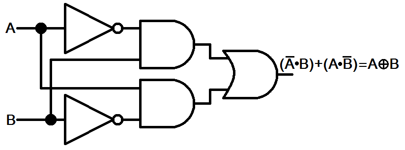
The truth table of an exclusive OR and exclusive NOR gate for two inputs is given in the table below.
| A | B | XOR | XNOR |
|---|---|---|---|
| 0 | 0 | 0 | 1 |
| 0 | 1 | 1 | 0 |
| 1 | 0 | 1 | 0 |
| 1 | 1 | 0 | 1 |
Examples of Simulating Digital Circuits using PSpice
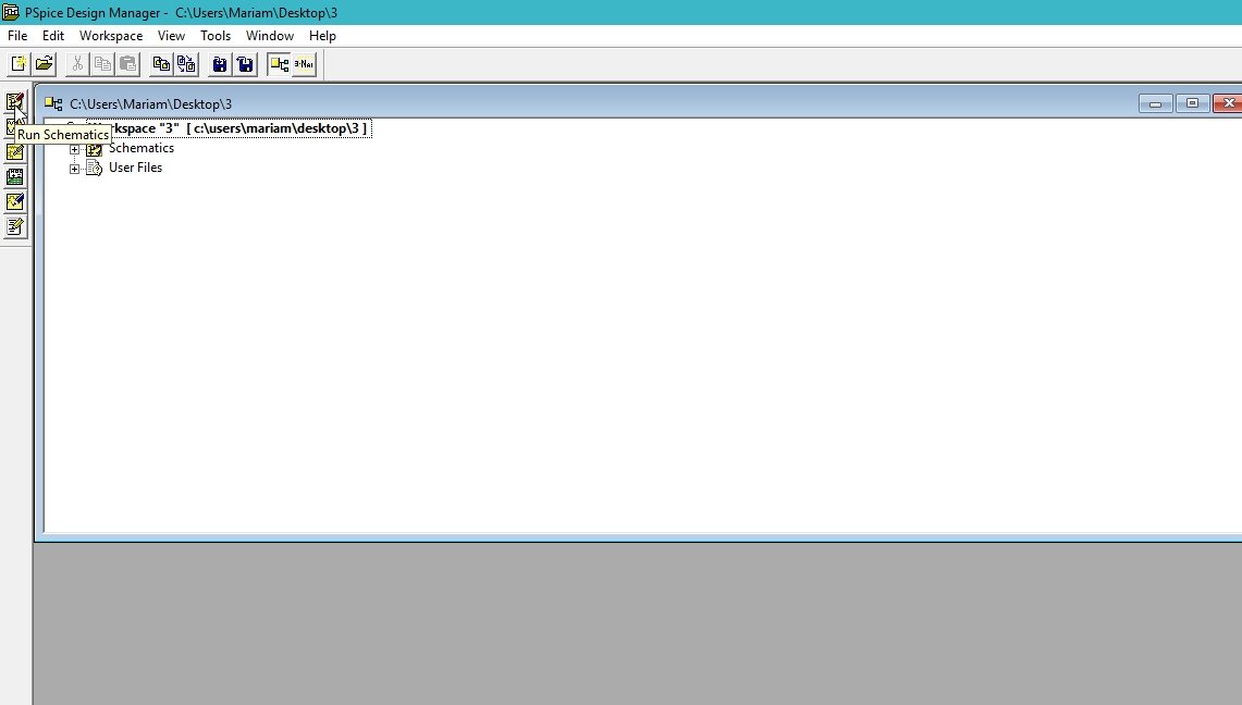
Let’s design a simple digital circuit, i.e., an exclusive OR circuit, and we will leave the exclusive NOR gate as an exercise. Open the PSPICE design manager on the PC by typing design manager in the search bar. From the design manager, click on the run schematic button to open a new blank schematic, as shown in the figure below.
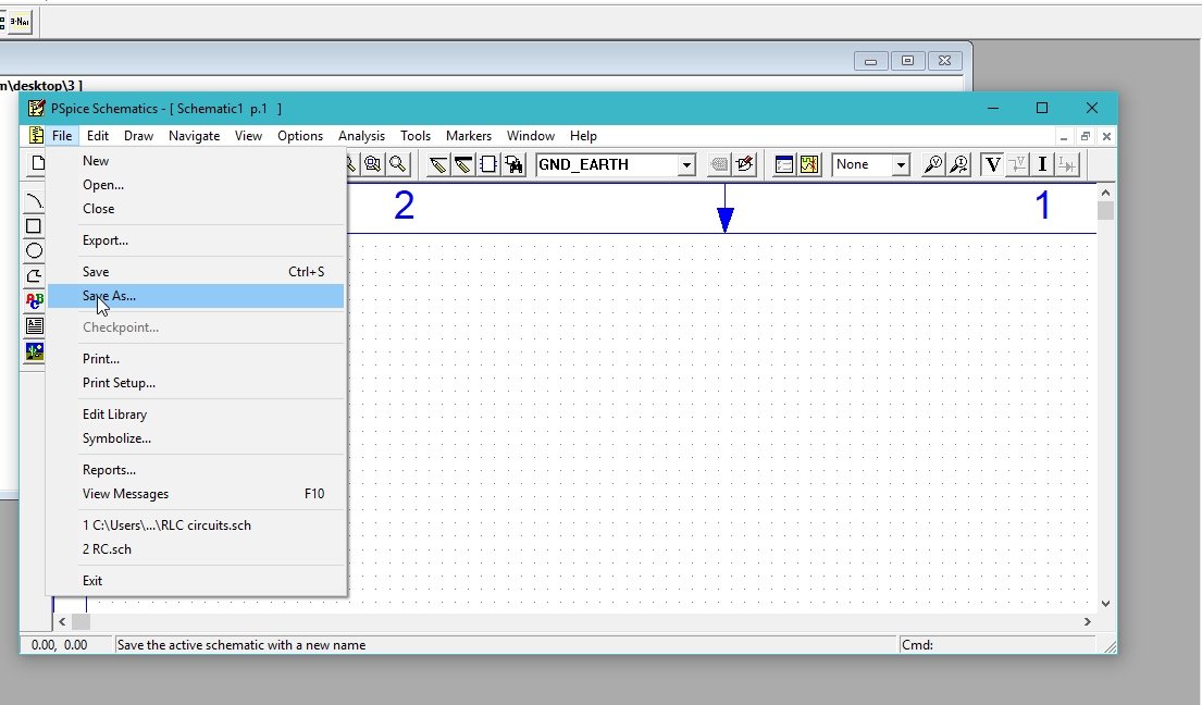
After opening the new schematic, before jumping into designing, first save the schematic by clicking on the file button at the top left corner and then selecting save as so that we can access it anytime in the future. Refer to the figure below.
Placing Components
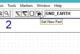
Click on the Get New Part icon at the top bar of the schematic window in order to search for the components that are needed for circuit design.
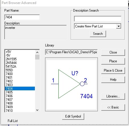
In the Get New Part window, type ‘7404’. It will display a NOT Gate available in PSpice. From that list, select a simple NOT gate, as shown in the figure below.
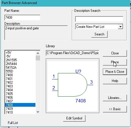
Again, open the Get New Part window, and in the part name block, type 7408. It selects the AND gate from the list given and then clicks on Place & Close, as shown in the figure below.
Again, open the Get New Part window, and in the part name block, type 7432. It selects the OR gate from the list given and then clicks on Place & Close, as shown in the figure below.

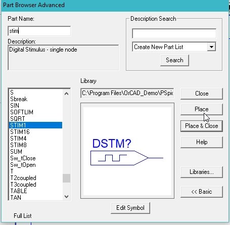
The next step is to place a ground, do the same again, and in the part name type stim and select the digital source, and then click on Place & Close, as shown in the figure below.
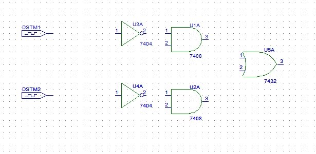
The components placed in the schematic window are shown in the figure below.
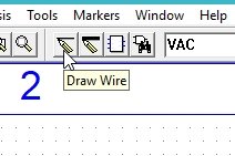
Click on the draw wire icon at the top bar of the schematic window in order to connect the already placed components for circuit design, as shown in the figure below.
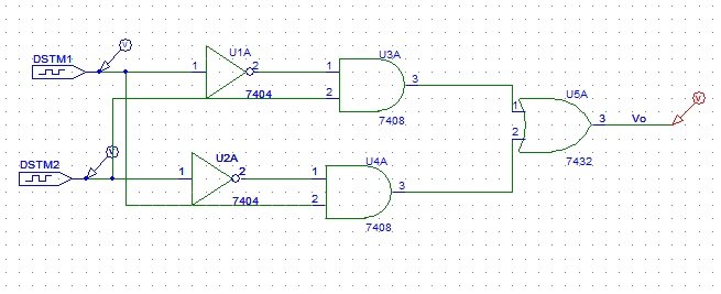
Complete Circuit Diagram
Connect all the components to complete the circuit diagram, as shown in the figure below.

On the top of the schematic window, click on the Voltage/Level Marker button, as shown in the figure below.

Place it at the output capacitor and at the input node, as shown in the figure below.
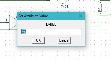
If we are interested in checking the voltage on a specific wire in spite of checking it at a node, double click on the wire, and in the window that appears as a result, we will type the name of the wire to label it with, as shown in the figure below.
Setting Input Attributes
The next step is to set the attributes of the input digital supply. Double-click on the dstm1 supply we connected in the circuit previously and set the input commands of the digital input system as shown in the figure below.
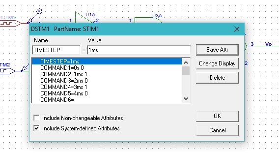
The commands in the attributes window represent the value of the input at the corresponding time in the command before the space. The COMMAND1 = 0s 0 shows that at time 0s the value of the input DSTM is 0, and the COMMAND2 = 1ms 1 shows that the value will update to 1 at time 1 millisecond. Similar is the case with COMMAND5 = 4ms 0, which means that at 4 milliseconds, the value of the input will be 0.
The next step is to set the attributes of the input digital supply. Double-click on the dstm2 supply we connected in the circuit previously and set the input commands of the digital input system, but these commands will not be the same as the commands of input 1, as shown in the figure below.
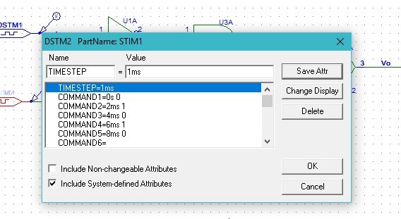
These commands will update after one complete cycle of the input 1 signal. After the input value of input source 1 changes from zero to one and then back to zero, the input value of input source 2 only changes from zero to 1. These commands are adjusted so that they complete all the binary input combinations for two variable inputs, as shown in the table below.
| A | B |
|---|---|
| 0 | 0 |
| 0 | 1 |
| 1 | 0 |
| 1 | 1 |
Simulation Setup
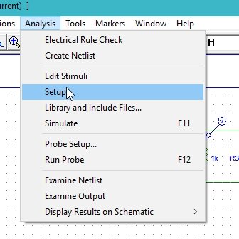
The next step is to adjust the properties of the simulations in order to produce a graph of the voltage at the marker. Click on analysis and then click on Setup, as shown in the figure below.
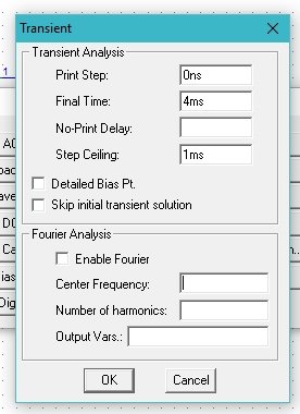
A window will appear. Click on the transient block on the window and adjust the properties of the window according to the requirements. Refer to the figure below.
Simulation
The final time of the response is 4 ms because we have set the commands for only 4 ms. Now comes the simulation part. Click on the analysis at the top bar of the schematic window and then click on simulate, as shown in the figure below.
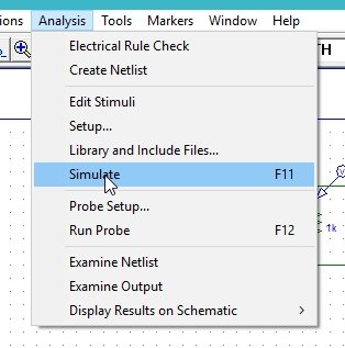
A schematic window will appear showing the voltage at the output wire and the input source, as shown in the figure below.
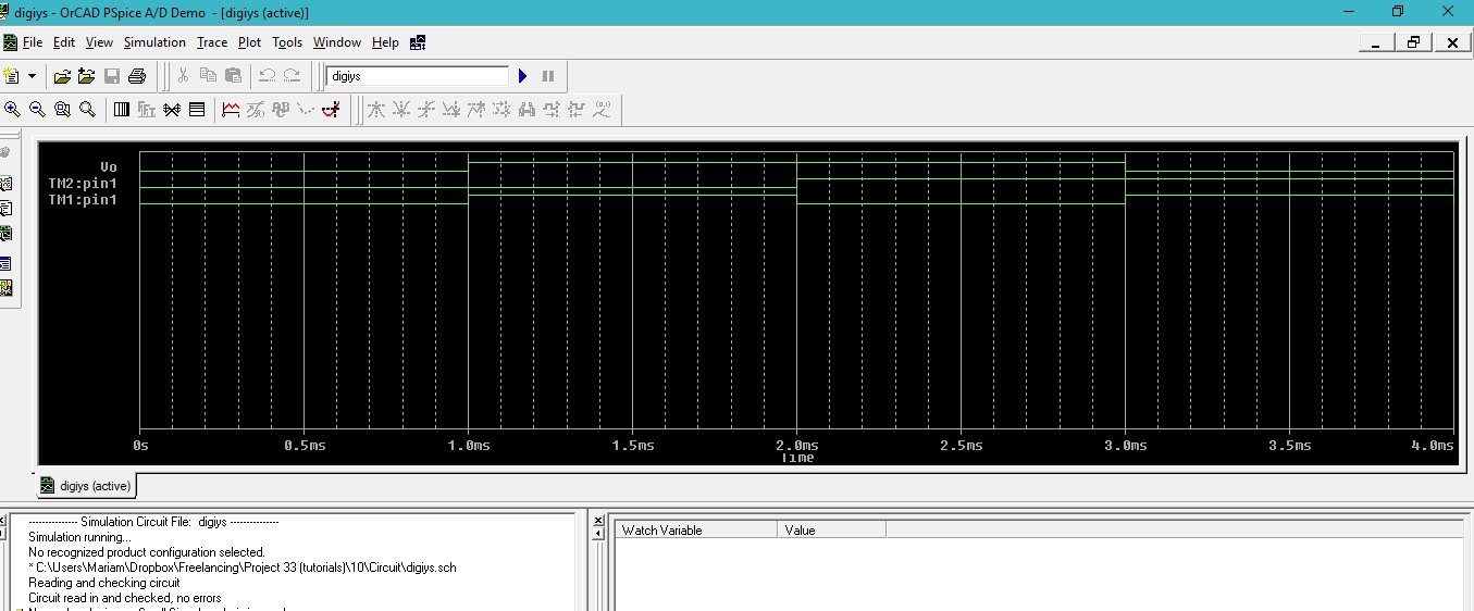
If we construct a table of the input values corresponding to the output values, the results will be similar to those discussed above. As is obvious from the figure above, the top-most wave is the output, and the lower two wave forms represent the inputs.
Exercise:
- Implement the XNOR gate using PSPICE and display the output along with the input.
(Hint: It is similar to the XOR gate with a not gate at the output.)
Conclusion
In conclusion, this tutorial provides an in-depth overview for designing and simulating digital systems in PSpice. It covers step-by-step procedures of example, with clear and concise explanation which helps us better understand the concept. You can utilize this and simulate more complex applications of digital systems. Lastly, an example is provided to reinforce the concept of digital systems in PSpice. Hopefully, this tutorial was helpful in expanding your knowledge of designing and simulating using PSpice.
You may also like to read:
- ESP32 with MPU6050 Accelerometer, Gyroscope, and Temperature Sensor ( Arduino IDE)
- PWM TM4C123 – Generate PWM Signals with Tiva C Launchpad
- IoT based Soil Moisture Monitoring System with ESP32 and Adafruit IO
- ESP32 BLE Server GATT Service Battery Level Indication
- How to use Conditional statements in Simulink : tutorial 6
- Telegram Control ESP32 and ESP8266 GPIOs and LEDs using Arduino IDE
This concludes today’s article. If you face any issues or difficulties, let us know in the comment section below.