This tutorial is about pinout reference of ESP8266 and different types of ESP8266 boards like Nodemcu, ESP01 , ESP12. First, I will give the overview of ESP8266 IC and its pinout and after that I will provide pinout reference of most popular ESP8266 boards.
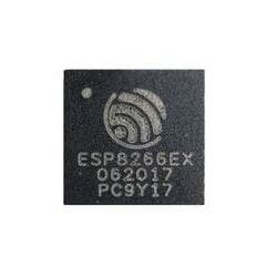
Esp8266 is a microchip in QFN package having capabilities of both TCP/IP suite and microcontroller. Esp8266 delivers highly integrated WiFi solution that meets the needs of the Internet of Things industries such as low cost, efficient power usage, trustworthy performance, and compact design. It is manufactured by Espressif Systems in Shanghai, China.
Having complete WiFi networking capabilities it can perform as a slave to a host microcontroller or as a standalone application. When we say the slave to a host microcontroller it means it can use as WiFi adaptor to any microcontroller using SPI or UART interfaces. While using as a standalone it can perform the capabilities of microcontroller and WiFi networking.

Esp8266 is based around Tensilica’s L106 Diamond series which is 32-bit processor and have on-chip SRAM. Also integrates power modules, RF balun, RF receiver and transmitter, analog receiver and transmitter, digital baseband, amplifier, filters, and some other minimal components.
Specifications of ESP8266
Esp8266 specification divides into three parts: Hardware, Software, and Wi-Fi. In hardware specification, its package size is QFN 32pins with a dimension of 5mm x 5mm. Operating voltages range from 2.5V to 3.6V. The chip consumes 80mA of current on average. Its CPU is Tensilica L106 which is a 32bit processor with on-chip SRAM. The peripheral interface contains UART, SDIO, SPI, I2C, I2S, IR remote control, GIPO’s, ADC, PWM, LED Light and button.
Its firmware can be updated using OTA and UART. It uses IPv4, TCP, UDP, and HTTP as network protocols. User can configure using AT commands set, Cloud Server and using a mobile application.
Wi-Fi frequency ranges from 2.4G to 2.5G. It uses standard Wi-Fi protocol IEEE 802.11 b/g/n. Esp6266 Wi-Fi capabilities are certified by Wi-Fi Alliance.
ESP8266 Chip Pinout and Descriptions
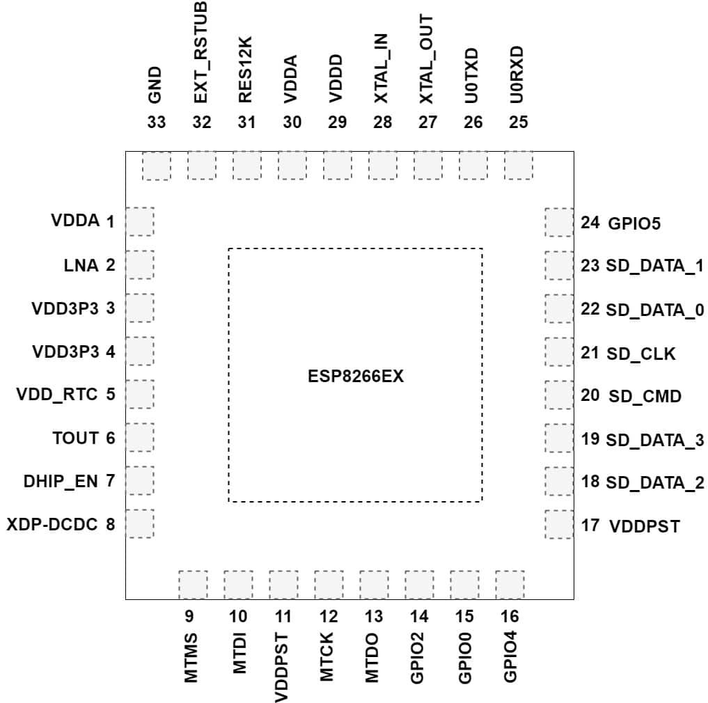
Pin layout of 32-pin QFN Package.
- Pin1: VDDA is a power pin for analog power ranges from 2.5V to 3.6V.
- Pin2: LNA is an input/output pin specifically used for RF antenna interface. Chip produces impedance of 39+j6 Ω.
- Pin3: VDD3P3 is a power pin to provide amplifier power ranges from 2.5V to 3.6V.
- Pin4: VDD3P3 is a power pin provide amplifier power ranges from 2.5V to 3.6V similar to pin3.
- Pin5: VDD_RTC is categorized as a power pin and supply 1.1V but this pin is not connected.
- Pin6: TOUT is an input pin functions as ADC pin to test the supply voltages of Pin3 and Pin4 and the input voltages of TOUT pin6. These two functions cannot perform simultaneously.
- Pin7: CHIP_EN I an input pin. When CHIP_EN pin is HIGH chip works properly when LOW chip consumed an only small amount of current.
- Pin8: XPD_DCDC is an input/output pin which is used to wake up the chip from deep sleep mode. Commonly it is connected with GPIO16.
- Pin9: MTMS is an input/output pin labeled as GPIO14 and it is used in SPI as clock pin (SPI_CLK).
- Pin10: MTDI is an input/output pin labeled as GPIO12 and it is used in SPI as Master-In-Slave-Out pin (SPI_MISO).
- Pin11: VDDPST is a power pin. It is a digital input/output power supply whose voltages ranges from 1.8V to 3.6V. Similar to pin17.
- Pin12: MTCK is an input/output pin labeled as GPIO13 and it is used in SPI as Master-Out Slave-In pin (SPI_MOSI) as well as used in UART as Clear To Send pin (UART_CTS).
- Pin13: MTDO is an input/output pin labeled as GPIO15 and it is used in SPI as Chip Select pin (SPI_CS) as well as used in UART as Request To Send pin (UART_RTS).
- Pin14: GPIO2 is an input/output pin used as UART TX during flash programming.
- Pin15: GPIO0 is an input/output used as Chip Select pin2 in SPI (SPI_CS2).
- Pin16: GPIO4 is an input/output pin purely used for input and output purposes.
- Pin17: VDDPST is a power pin. It is a digital input/output power supply whose voltages ranges from 1.8V to 3.6V. Similar to pin11.
- Pin18: SDIO_DATA_2 is an input/output pin labeled as GPIO9 and used to connect with data pin 2 of SD card.
- Pin19: SDIO_DATA_3 is an input/output pin labeled as GPIO10 and used to connect with data pin 3 of SD card.
- Pin20: SDIO_CMD is an input/output pin labeled as GPIO11 and used to connect with command pin of SD card
- Pin21: SDIO_CLK is an input/output pin labeled as GPIO6 and used to connect with the clock pin of SD card.
- Pin22: SDIO_DATA_0 is an input/output pin labeled as GPIO7 and used to connect with data pin 0 of SD card.
- Pin23: SDIO_DATA_1 is an input/output pin labeled as GPIO8 and used to connect with data pin 1 of SD card.
- Pin24: GPIO5 is an input/output pin purely used for input and output purposes.
- Pin25: U0RXD is an input/output pin labeled as GPIO3 and used as UART RX during flash programming.
- Pin26: U0TXD is an input/output pin labeled as GPIO1 and used as UART TX during flash programming. Also used as SPI Chip Select pin 1 (SPI_CS1).
- Pin27: XTAL_OUT is classified as an input/output pin and connected to the output of the crystal oscillator.
- Pin28: XTAL_IN is classified as an input/output pin and connected to the input of the crystal oscillator.
- Pin29: VDDD is a power pin provide analog power ranges from 2.5V to 3.6V.
- Pin30: VDDA is a power pin provide analog power ranges from 2.5V to 3.6V. Similar to pin29.
- Pin31: RES12K is an input pin which is serial connected with 12 kΩ resistors and connected to the ground.
- Pin32: EXT_RSBT is an input pin used to rest the chip by providing an external reset signal which is active at a low voltage level.
- Pin33: GND is a power pin acts as a ground for the chip.
All GPIO’s can be used as Input and Output pin but they also have their specific function.
Schematic
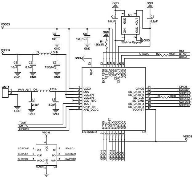
ESP8266 schematics include the following components:
- Power supply
- Power-on sequence and reset
- Flash
- Crystal oscillator
- RF
- External resistor
- UART
So far we cover Esp8266 preamble, functional block diagram, pins layout, description, and schematics.
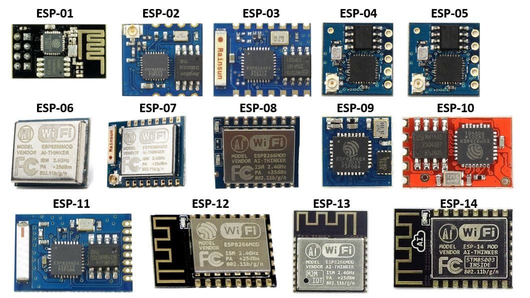
In August 2014 Espressif Systems launched their first raw module which is manufactured by third part AI-Thinker and module referred as ESP-01 module. Since then Ai-Thinker developed a series of modules based around ESP8266, this series referred as ESP-xx modules ranges from 01 to 14.
Pinout of different types of ESP8266 Modules
In this section of article, we will talk about pinout of different versions of ESP8266 module starting from ESP-01 to ESP-12.
Espressif Systems released their first official software development kit to program the chip directly without interfacing with an external microcontroller. Since then there are many official SDKs but Espressif maintain only two SDKs stable one is based on FreeRTOS and other based on callbacks. There is also a variety of open source SDK’s for ESP8266.
Arduino: is the most commonly used SDK due to its popularity. It is a C++ based SDK. ESP6266 is easy programmed as Arduino boards. The core files are available on GitHub.
NodeMCU: is a Lua Based software development kit.
MicroPython: is the use of python language for embedded devices.
Espruino, Mongoose OS, uLisp, Sming, Platform IO, ESP Easy, Smick, ESP Open RTOS are some other open source SDK’s.The need for these development boards is required due to ESP-xx modules series lacks on-board a voltage regulator, USB to UART Bridge like CH340G and Silicon Lab’s CP2102 and micro USB connector. Before we had to buy voltage regulator and USB to UART bridge separately and then wired them up with ESP-xx modules to flash it.
Here we will discuss mostly development board based around ESP-12E module.
ESP8266 12E Module Pinout
Esp8266 12E module has a total 22 pins which include
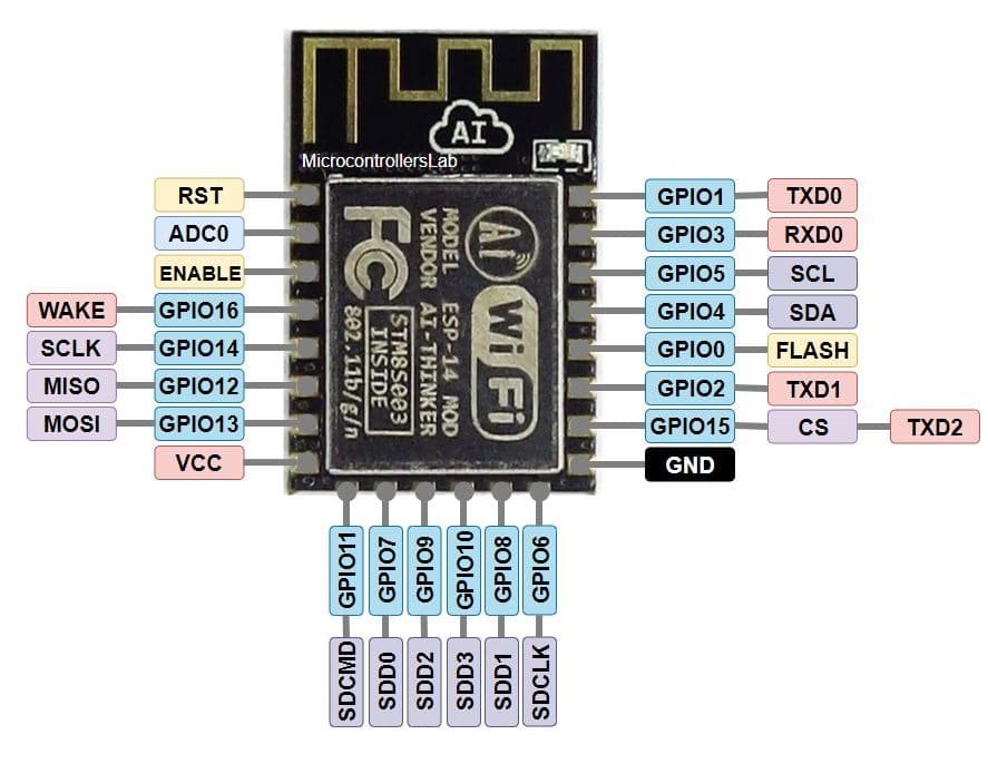
| No. of Pins | Pin Label | Description |
|---|---|---|
| 17 | GPIO | GPIO pins range from GPIO0 to GPIO16 includes SPI, I2C, SDIO, UART interface pins. |
| 1 | ADC | 10 bit Analog to Digital Converter. |
| 1 | VCC | Supply Voltage 3.3V |
| 1 | GND | Ground pin |
| 1 | RST | Rest Pin |
| 1 | Enable | Chip Enable Pin |
ESP8266 12E Wemos D1 Mini pinout
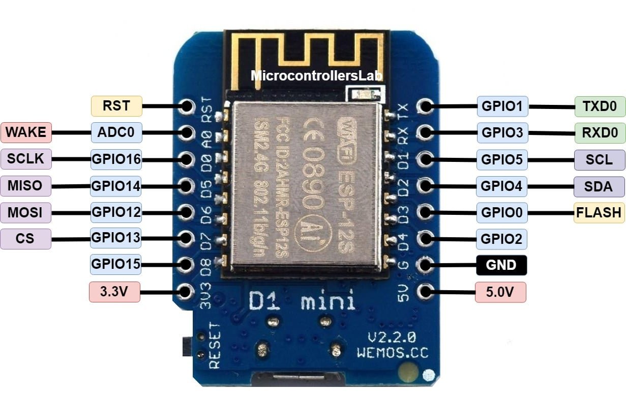
Wemos D1 Mini development board has a total 16 pins in which 12 pins are active, uses ESP-12 module, onboard reset button, 3.3 voltage regulator, Micro USB, USB to UART bridge and some other components.
| No. of
Pin | Label | Description |
|---|---|---|
| 1 | 3.3V | 3.3 volts pin |
| 1 | 5.0 | Input 5V voltage pin |
| 1 | GND | Ground pin |
| 1 | ADC | 10 bit Analog to Digital Converter |
| 1 | RST | Reset Pin |
| 9 | D0 to D8, | Input/output pins also used for SPI and I2C, Flash. |
| 2 | RX,TX | UART interface. |
ESP8266 01 Module pinout
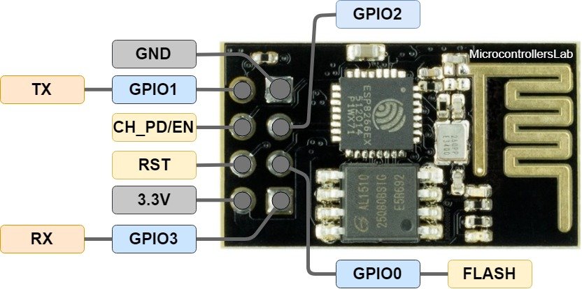
ESP8266 01 Module is different but commonly as used as the above development boards. This board is not breadboard friendly often separate programming module is used for programming. It has a total 8 pins in which 6 pins are active.
| No. of
Pin | Label | Description |
|---|---|---|
| 1 | 3.3V | Supply 3.3 volts pin |
| 1 | GND | Ground pin |
| 1 | RST | Reset Pin |
| 1 | CH_PD/EN | Chip Power and Enable pin |
| 4 | GPIO 0 to 3 | UART interface and input/output pins |
ESP8266 12E NodeMCU Development Board pinout

NodeMCU development board has a total 30 pins in which 14 pins are active, uses ESP-12 module, onboard reset and flash button, 3.3 voltage regulator, Micro USB, USB to UART Bridge and some other components.
| No. of
Pin | Label | Description |
|---|---|---|
| 3 | 3.3V | 3.3 volts pins |
| 1 | Vin | Input 5V voltage pin |
| 4 | GND | Ground pins |
| 1 | ADC | 10 bit Analog to Digital Converter |
| 1 | RST | Reset Pin |
| 1 | EN | Chip Enable pin |
| 1 | CLK | CLK pin for SPI and SDIO interface |
| 1 | SD0 | Data pin 0 for SDIO and MISO pin for SPI Interface. |
| 1 | CMD | Command pin for SDIO interface and Chip select pin for SPI interface. |
| 1 | SD1 | Data pin 1 for SDIO interface and MOSI pin for SPI Interface. |
| 1 | SD2 | Data pin 0 for SDIO interface and also used as GPIO9. |
| 1 | SD3 | Data pin3 for SDIO interface and also used as GPIO10. |
| 2 | RSV | Reserved pins. |
| 11 | D0 to D8, RX, TX | Input/output pins also used for UART, SPI, I2C, Flash and wake pin. |
ESP8266 Peripherals
The ESP8266 have the following peripherals:
- 17 General Purpose Input Output Pins
- Serial Peripheral Interface (SPI)
- Inter-Integrated Circuit (12C)
- Inter-IC Sound interfaces (12S) with Direct Memory Access
- Universal Asynchronous Receiver Transmitter interface.
- 10-bit Analog to Digital Converter
Analog Input
ESP8266 have an only one 10-bit analog to digital converter that referred as ADC0 and labels as A0. But this is also its one of the biggest disadvantage because mostly user have to connect two sensors so we have to buy separate ADC modules, IC and multiplexing circuit to interface two or more sensors but this is a topic of another article.
Input analog voltage of ESP-01 module ranges from 0 to 1V. Development board based around ESP-12E module have input analog voltage ranges from 0 to 3.3V. So we have to keep in mind while writing a sketch to use A0 pin.
PWM Pins
The ESP8266 allows PWM in all input/output pin from GPIO0 to GPIO16. PWM signals have 10-bit resolutions.
SPI Pins
A Serial Programming interface (SPI) has following pins in ESP8266
- GPIO12 for Mater-Out-Slave-In (MOSI)
- GPIO13 for Mater-In-Slave-Out (MISO)
- GPIO14 for Serial Clock (SCLK)
- GPIO15 for Chip Select (CS)
I2C pins
ESP8266 provide only software I2C interface it means we can use any two pins for I2C but following pins mostly used.
GPIO5 for Serial Clock Line (SCL)
GPIO4 for Serial Data Line (SDA)
Interrupt Pins
We can use any GPIO pin for interrupts except GPIO16.
Wake Up
To wake up ESP8266 from deep sleep using GPIO16 by connecting it to RST pin. This is a topic for another article.
On board LED
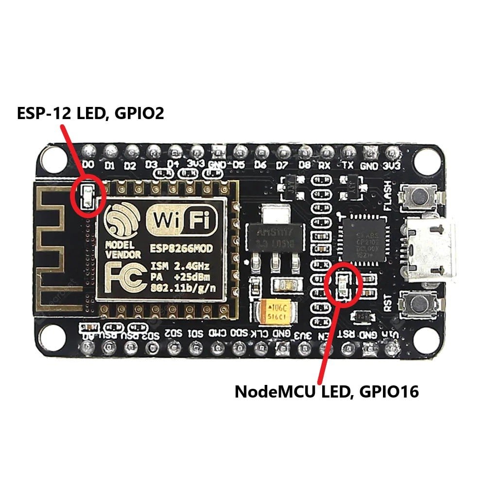
Mostly development boards have one or more built-in LEDs. The LED built on the ESP8266 module is connected to GPIO2 and the LED built on development board connected to GPIO16.
Reset and Flash Button
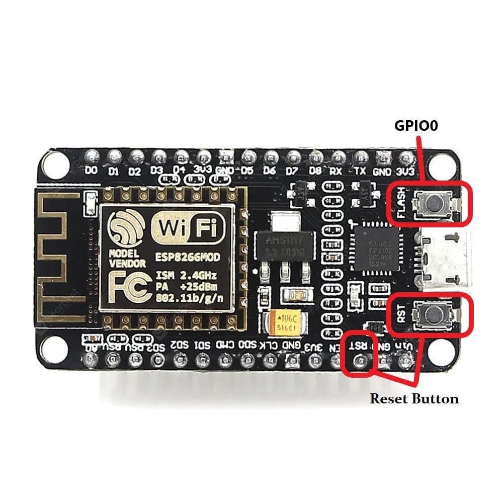
Pressing the reset button or pulling RST pin low resets the ESP8266 chip. Pressing the Flash button or pulled the GPIO0 low sets the ESP8266 chip into bootloader mode.
Which pin of ESP8266 to use
Always keep in mind that GPIO label does not match the label on the silkscreen. For example GPIO0 corresponds to D3 and D0 corresponds to GPIO16. The GPIOs with a green tick is best to use.
| Label | GPIO | Input | Output | Description |
|---|---|---|---|---|
| A0 | ADC0 | Analog Input | No | For analog input from 0 to 3.3v and no output. |
| RX | GPIO3 | Yes | RX pin only | High at Boot. |
| TX | GPIO1 | Tx pin only | Yes | High at Boot. |
| D0 | GPIO16 | No interrupt | No I2C, PWM | Used to wake up chip from deep sleep, High at Boot. |
| D1 | GPIO5 | Yes | Yes | Often used as SCL |
| D2 | GPIO4 | Yes | Yes | Often used as SDA |
| D3 | GPIO0 | Pulled up | Yes | Connected to Flash button |
| D4 | GPIO2 | Pulled up | Yes | Connected to built-in LED, High at Boot. |
| D5 | GPIO14 | Yes | Yes | SCLK pin for SPI interface |
| D6 | GPIO12 | Yes | Yes | MISO pin for SPI interface |
| D7 | GPIO13 | Yes | Yes | MOSI pin for SPI interface |
| D8 | GPIO15 | Pulled to ground | Yes | CS pin for SPI interface |
ESP8266 pin High and Low-voltage signal at Boot
While booting ESP8266 the following pins provide 3.3v signal on specified pins so connecting relays, transistor or any other peripheral devices can misbehave. The following pin output 3.3v signal on Boot:
- GPIO16
- GPIO3
- GPIO1
- GPIO10
- GPIO9
All other GPIOs pin provide low voltage single on Boot except GPIO4 and GPIO5. So the GPIO4 and GPIO5 are the best pins to connect relays, transistor and other peripheral devices to stable results.
Pins Configuration during Boot
To boot the ESP8266 successfully we have to disallow the specified pins to get HIGH or LOW.
- GPIO16: pin is high at BOOT
- GPIO3: pin is high at BOOT
- GPIO10: pin is high at BOOT
- GPIO9: pin is high at BOOT
- GPIO2: pin is high on BOOT, boot failure if pulled LOW
- GPIO1: pin is high at BOOT, boot failure if pulled LOW
- GPIO0: boot failure if pulled LOW
- GPIO15: boot failure if pulled HIGH
Applications of ESP8266
- Home automation
- Smart plugs and switches
- Home appliances (like AC, Printer)
- Wireless industrial control
- Sensor Devices
- Wearable Gadgets
- IP cameras
- Security ID tags
- Wi-Fi location-aware devices
- Wi-Fi position system
You may also like to have a look into other ESP8266 tutorials:
You have a mistake on your pinout pic – all SPI pins are wrongly marked – moved by one pin up than they should
Thanks for the correction
“The GPIOs with a green tick is best to use.”
(There are no green ticks)…..
PS thanks for the useful info 🙂
Hi. I came here to try to differentiate the chips, but I’m still confused as ever. My module (Bought on Ali Express, cheap asf). It sort of looks like ESP 07, but have the shielding of ESP 12.
I didn’t see any notes on that “AI Thinker” which it says on a few modules.
I have the NodeMCU, version 1 I think, less important. It does however have that AI-deal on it, whilst my Ali-bought does not, and is also loose PCB’s, like ESP 12, with an additional exception that it has both the antenna outlet and what appears to be an elongated SMD antenna (Like 07).
What is the difference, and are these product images of yours in need of an update?
Once we give low input to pin 16 of NodeMCU ESP8266, it remains low, see my code below which is not able to switch off led because of this issue, can’t we use pin 16 as general purpose input?
See my complete code
https://github.com/mrnams/IOT/blob/main/ESP8266/Examples/Basic/One-Led-Two-Push-Buttons
Cant you please put an arrow pointing specifically to PIN 11 ? It is mentioned, but I don’t see number 11’\.Thanks.
“GPIO1: pin is high at BOOT, boot failure if pulled LOW”
I’m not finding this to be true on my ESP-12E. AFAIK only GPIO 0, 2, and 15 control boot mode.
Hello. Do you have sample wiring and program for ESP8266 and TB6612FNG motor driver?
Hi.
I found a mistake in the pinout of ESP8266 12E Wemos D1 Mini:
The labels on left side have to be moved down by one pin:
WAKE = GPIO16,
SCLK = GPIO14
MISO = GPIO12
MOSI = GPIO13
CS = GPIO15
Regards, Gerrit.