74LS14 is a Schmitt trigger hex 8-bit inverter IC. In electronics devices, Schmitt Trigger is one the comparator-based circuit which gives the output on the based the previous output. In Schmitt Trigger the input value can be analog or digital but the output will be in two forms 1 or 0. Any circuit is convertible to Schmitt trigger by applying a positive feedback system. In this circuit, the threshold is being used to get output. When the value is higher than the threshold the output will be HIGH otherwise it will be considered in the LOW state. These circuits are not only used to convert analog to digital, but it also helps to remove the noise from the signal.
The Schmitt Trigger comes in two types, one is inverting and the second is not inverting. In non-inverting, the output comes HIGH at the peak of the input signal and LOW at the minimum amplitude of the signal. In inverting the signal gets inverted, it gives LOW at the peak and HIGH at the minimum amplitude of the signal. There are multiple devices and circuits for non-inverting signal but here we will discuss the inverting one.
Recommended Components
The following parts are used in this article, along with a generic electronics kit that is handy for building and testing the circuit.
| Component | How it’s used | Buy on Amazon |
|---|---|---|
| 74LS14 Schmitt-trigger hex inverter | The 74LS14 Schmitt-trigger hex inverter this article covers. | Check Price |
| Electronic component assortment kit (1390 pcs) | A handy assortment of resistors, capacitors, LEDs, diodes and transistors for building circuits. | Check Price |
| Digital multimeter (AstroAI) | Measures voltage, current, resistance and checks continuity while you build and debug. | Check Price |
| Breadboard | Solderless base for prototyping the circuit. | Check Price |
| Jumper Wires | Make the connections on the breadboard. | Check Price |
As an Amazon Associate we earn from qualifying purchases. Prices and availability are accurate as of the date/time indicated and are subject to change.
Introduction to 74LS14 IC
There is an IC name 74LS14 is used as an inverting Schmitt trigger. It comes up with six triggers that can be used easily. The single Schmitt trigger circuit may seem larger in size but the IC has a smaller size and also comes in multiple packages. IC 74LS14 uses a single power supply to all the triggers and can be used to operate with any TTL based device. These circuits can be easily operated in any environment and can be triggered easily with the slowest input ramps.
Pin Diagram 74LS14
The pinout of this integrated circuit is similar to 74LS04. However, the functionality difference is due to a Schmitt trigger function.
Figure 1: PINOUT
74LS14 Pin Configuration Details
| PINS | DETAIL | |
|---|---|---|
| 1A | Pin 1 | Pin 1 will be used as the input pin for the first Schmitt trigger. |
| 1Y | Pin 2 | Pin 2 will be as the output pin of the first Schmitt trigger. |
| 2A | Pin 3 | Pin 3 will be used to give the input at second Schmitt trigger. |
| 2Y | Pin 4 | Pin 4 will be used to receive the output of the second Schmitt trigger. |
| 3A | Pin 5 | Pin 5 will be used to give the input at third Schmitt trigger. |
| 3Y | Pin 6 | Pin 6 will be used to receive the output of the third Schmitt trigger. |
| GND | Pin 7 | Pin 7 will be used as the common ground to use the devices IC with other devices. |
| 4Y | Pin 8 | Pin 8 will be used to receive the output of the forth Schmitt trigger. |
| 4A | Pin 9 | Pin 9 will be used to give the input to the forth Schmitt trigger. |
| 5Y | Pin 10 | Pin 10 will be used to give receive the output from the fifth Schmitt trigger. |
| 5A | Pin 11 | Pin 11 will be used to use to give the input to fifth Schmitt trigger. |
| 6Y | Pin 12 | Pin 10 will be used to receive the output from the sixth Schmitt trigger of IC. |
| 6A | Pin 13 | Pin 11 will be used to give the input to the sixth Schmitt trigger. |
| VCC | Pin 14 | VCC pin will be used to give the power to the IC to make it functional. |
74LS04 Hex NOT Gate IC
74LS02 Quadruple 2-Input NOR Gate IC
Schmitt trigger Working
The switching between the HIGH and LOW signal in a single Schmitt trigger will happen very quickly but it will happen with the specific method. The rise and fall time for IC describe how much time IC will take to give the new output. Here in 74LS14 IC, the output will be change within 12ns. If the input is given to the IC then it will take 12 ns to give the output, it doesn’t matter the output is LOW or HIGH. Here we are using the inverter Schmitt trigger so If the input voltages are lower or equal to the hysteresis voltages then the output will be HIGH and after 12ns if the voltages changes then at the end of 12 ns the output will depend on the input signal again, this cycle continues until we stop the circuit.

Figure 2: THRESHOLD WORKING
The input circuit will be of three types. Digital, Sin wave and noisy sine wave. Here we will learn how each signal will be handled by the IC. First, use the sign wave as the input signal. When the input signal will be at peak then the output will at LOW and when input will be at lower the threshold then the output will be at its peak in IC. The same will happen with a slow edge signal.

Figure 3: SIN WAVE

Figure 4: SMOOTH EDGE
In the case of the noisy signal, the amplitude of the signal will change like sign wave and slow edge wave but at some point, it will cause both LOW state and HIGH state within a few microseconds. The signal will get inverted in the digital signal but in the digital signal, the output will also be with Noise, that’s why in Schmitt triggers the noise gets immunity due to its fast speed.

Figure 5: NOISY SIGNAL
Examples 74LS14
In this example, we will use one of the Inverter with a sign wave signal and then we will get the output in the oscilloscope. First, we will understand what should be the output. When we will give the sign wave to the inverter then the first output will be in digital form and second its output will depend on the input signal frequency. If the signal is changing with faster frequency then we will receive multiple square waves in the specific interval. Here I will use 50 Hz and see what is the output and how much waves we are getting. First, design the circuit as shown in the below image.

Figure 6:PROTEUS CIRCUIT

Figure 7: OUTPUT WITH 50 HZ
As we can view in the image the sign wave is converted into the digital wave and we are getting only one digital wave on the specific time interval. Let’s change the frequency and visualize the output.
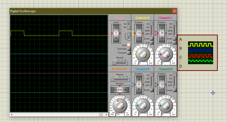
Figure 8: OUTPUT with 100HZ
Here we can see when we change the input frequency from 50Hz to 100 then output waves turned from one to two. It is because the speed of the IC remains constant but when we change the frequency the frequency starts shifting much faster than before that we start receiving two times change in frequency from peak to low and low to peak within 1ms. This example will go the same for a smooth edge signal but we can understand noise immunity here better.
Here we can see the shift of the sign wave increase due to the change in frequency. In noisy signal at some point when the signal reaches the threshold, the output starts converting fluctuating between HIGH and LOW. This gives the noisy signal and the upper hand. We can remove these kinds of effects with other devices but a single inverter doesn’t have the feature to remove that noise.
74LS14 APPLICATIONS
- It is used in industrial stepper motors.
- It has wide use in Power meter and Power analyzers.
- Digital input modules also use 74LS14 for factory automation.
- In outdoor units of Air conditions for residential ductless also comes up with 74LS14.
- The IC can be used for Noise Removing.
- It can also be used as a Dead band Filter.
- IC 74LS14 can also be used as a Hysteresis controller and Debouncing circuits.
FEATURES
- It can be used as a HEX inverter.
- It can be operated with a very slow change in amplitude.
- It can be used as a noise impunity device.
- It comes in multiple packages with all 14-Pins, SO, SSOP, SOIP, and PDIP.
SPECIFICATIONS
- It is operated able at 5V but the voltages can be increased to 7 Volts max.
- The device comes in two-level hysteresis voltages, the low hysteresis voltages are 0.25V and High hysteresis voltages are 3.4V.
- The Max output current for IC is 8.0mA and Minimum will be -0.4mA
- The Rise and Fall time of the IC is 12 ns