74LS93 or SN74LS93 is a 4-bit binary counter. Counters have a major role in every electronics device. The output of the counters can be used in multiple devices as pulse counting or for generating interrupts, etc. Counters come up in two form Asynchronous and Synchronous counters. Both these types of counters use the flip flops to count the binary digits.
Recommended Components
The following parts are used in this article, along with a generic electronics kit that is handy for building and testing the circuit.
| Component | How it’s used | Buy on Amazon |
|---|---|---|
| 74LS93 4-bit binary counter | The 74LS93 4-bit binary counter IC this article covers. | Check Price |
| Electronic component assortment kit (1390 pcs) | A handy assortment of resistors, capacitors, LEDs, diodes and transistors for building circuits. | Check Price |
| Digital multimeter (AstroAI) | Measures voltage, current, resistance and checks continuity while you build and debug. | Check Price |
| Breadboard | Solderless base for prototyping the circuit. | Check Price |
| Jumper Wires | Make the connections on the breadboard. | Check Price |
As an Amazon Associate we earn from qualifying purchases. Prices and availability are accurate as of the date/time indicated and are subject to change.
Introduction to 74LS93 Binary Counter IC
Here we will discuss 74LS93 which is a four-bit counter. It consists of 4 JK flip flops which act on the input pulse no matter how we gave the input pulse. We can use the microcontroller or timer IC for pulse input. The 74LS93 IC comes up with two reset pins, two clock pins, and four output pins. The IC is made up of two counters one is mod 2 counter another one is mod 8 counter. The whole IC gives the output 4 bits which counts from 0 to 15 in binary. This is compatible with any microcontroller or TTL based devices. It comes in multiple packages such as DIP, SMD with all 14-pins. The 74L93 binary counter comes up with internal protection from high-speed termination.
74LS193 Pinout Diagram

Figure 1: Pin Configuration
Pin Diagram Configuration
| PINS | DETAIL | |
|---|---|---|
| ~CP1 | Pin 1 | The IC consist of multiple mod counters, The Pin 1 is used to give the pulse to mod eight counter. It’s an active LOW pin. |
| MR1 | Pin 2 | Pin 2 is a reset pin used to reset the counter in case of any requirement. It’s an active HIGH pin. |
| MR2 | Pin 3 | Pin 3 is the second reset pin used to reset the counter. It’s an active HIGH pin. |
| NC | Pin 4 | Pin 4 is known as NC (no connection) pin which doesn’t have any role in the internal circuit of the IC. It can be used to the PCB for proper support of IC with the board. |
| VCC | Pin 5 | Pin 5 is a power pin used to power up the IC to make it functional. |
| NC | Pin 6 | Pin 6 and Pin 7 are also the NC pins of the IC. |
| NC | Pin 7 | |
| Q2 | Pin 8 | Pin 8 is an output pin of the IC. The actual output comes in 4 pins and Pin 8 gives the third bit of 4-bit binary data. |
| Q1 | Pin 9 | Pin 9 is also an output pin. It gives the second bit of the 4-bit binary data. |
| GND | Pin 10 | Pin 10 is a ground pin. It is used to make the IC ground common with the other compatible devices to make it functional with them. |
| Q3 | Pin 11 | Pin 11 is also an output pin. It gives the first bit of the 4-bit binary data. |
| Q0 | Pin 12 | Pin 12 is also an output pin. It gives the last bit of the 4-bit binary data. |
| NC | Pin 13 | Pin 13 is also the NC pins of the IC. |
| ~CP0 | Pin 14 | Pin 14 is the second input pin of the IC. It uses to give the pulse to the mod two counter in the IC. This pin is directly connected to the clock of JK flip flop of Q0. |
Other Equivalents are 74LS192, 74HC19, 4516
Other Counters ICs: CD4020, CD4022, CD4060, CD40102, CD4017, CD4026, 74LS93
74LS93 Binary Counter Features
- It can be used as a simple 4-bit counter.
- It comes in multiple packages with all 14-pins, PDIP, GDIP and PDSO.
- The clock pulse can be provided by timers such as 555 timers or any microcontroller.
- The IC has a faster speed to almost 32MHz.
- The output of the 74LS93 counter comes in TTL, which makes it compatible with other ICs and microcontrollers.
Electrical Specifications SPECIFICATIONS
- The operating voltage range for IC is 4.5 to 5.5V, but typical Operating Voltages are 5 Volts
- The HIGH and LOW states will be represented by voltages on the IC. The HIGH will be represented by 3.5V (min) and LOW will represent by 0.25V (min)
- The output for the current will also be different from IC. The HIGH state current will be -0.4mA and LOW will be 8mA
- The clock input frequency for CP0 is 32MHz and CP1 is 16MHz
- The pulse width for CP0 will be 15ns and for CP1 will 30ns, it will be double also like input frequency
- The operating temperature range can also be from 0 to 70 degrees
Note: Further details on electrical features and specifications are available in the datasheet.
How does 74LS93 Digital Counter Works?
The pins we are going to use for the 74LS93 binary counter are two input pins, two reset pins, and four output pins. First, connect the powers and then connect the first clock pin (Pin 1) with the last bit (Pin 12) . We will discuss later why we did that. After that connect the reset pins with the ground. In other cases when we need to control the reset then pins configuration for reset pins will be different. After that connect the second clock pin (Pin 2) with the output of timer or any other pulse generate to change the output. After that, we can use the IC to get the output on Pin 8, 9, 11 and 12. Here’s the circuit diagram.

Figure 2: Circuit Diagram
The input circuit will be made of two parts, one is MOD 2 counter and the second is the MOD 8 counter. The mode two counter gives the output only 1 and 0 when the clock pulse input changes from HIGH to LOW. The MOD 8 counter contains three JK flip flops and every flip flop receives the clock pulse from the previous output of JK Flip Flop. The output of MOD 2 goes to the clock pulse of the first JK flip flop of MOD 8. Every JK Flip Flop output consider as the output bit which makes the total 4 bits here.
Internal Circuit Diagram 74LS93
First, take a look at the internal circuit for proper understanding.
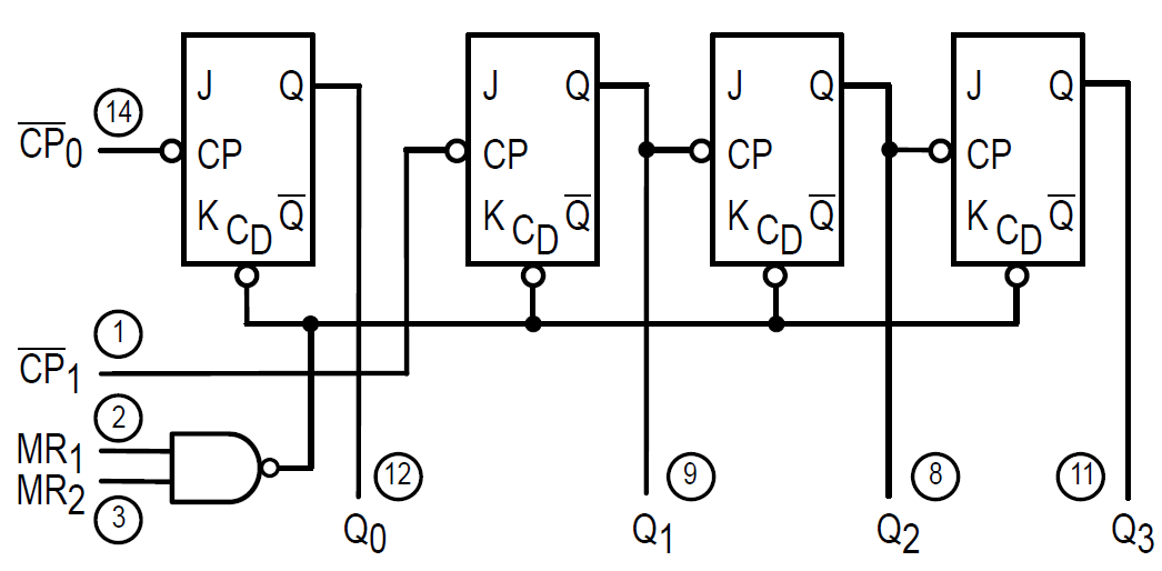
Every JK flip flop gives only 1 and 0 states. Every JK Flip flop changes its state whenever the previous Flip Flop output becomes LOW from HIGH, but the first flip flop doesn’t connect to the second one, so that why we connect the first clock pin (CP1) with the output of the first flip flop of MOD 8 counter. This four flip flop circuit in series while receiving the clock pulse from previous output makes the output to start from 0000 to 1111 and then come back to 0000 after reaching 1111 once. Every binary bit will represent the number of a binary decimal and it will happen in series. Here’s the table of every decimal number related to binary decimal number.
| COUNTING | OUTPUT | |||
|---|---|---|---|---|
| Q3 | Q2 | Q1 | Q0 | |
| 0 | 0 | 0 | 0 | 0 |
| 1 | 0 | 0 | 0 | 1 |
| 2 | 0 | 0 | 1 | 0 |
| 3 | 0 | 0 | 1 | 1 |
| 4 | 0 | 1 | 0 | 0 |
| 5 | 0 | 1 | 0 | 1 |
| 6 | 0 | 1 | 1 | 0 |
| 7 | 0 | 1 | 1 | 1 |
| 8 | 1 | 0 | 0 | 0 |
| 9 | 1 | 0 | 0 | 1 |
| 10 | 1 | 0 | 1 | 0 |
| 11 | 1 | 0 | 1 | 1 |
| 12 | 1 | 1 | 0 | 0 |
| 13 | 1 | 1 | 0 | 1 |
| 14 | 1 | 1 | 1 | 0 |
| 15 | 1 | 1 | 1 | 1 |
The timing diagram of all output signals from Q0-Q3 on every edge of the clock signal is shown here.

74LS93 Example one
In this example, we will use the IC to count the binary counting. First design the circuit in proteus with logic states. We are going to use the momentary action logic input for clock input. When we will give the clock pulse to the IC it changes the output to the further binary number. This process will happen in the series. Here’s the circuit and its initial state will be 0000 without doing any input pulse to the circuit.

Whenever we change the pulse to the circuit the input changes to the next number. This process will happen continuously from 0000 to 1111 and then again from 0000 until we are changing the clock pulse. This counting method is easy to implement and easy to use with any TTL Device or Microcontroller.
74LS93 Single Digit Counter Example
In this example, we used two 74LS20 ( 4 input NAND gate) and 3 Not gates 74LS04 to design a decimal counter with BCD seven-segment display. This decimal counter counts from zero to nine. Although, 74LS93 is a 4 bit counter and it can counter from 0-16 in binary and we can use two seven-segment displays to show counter values.
We have used only one 7-segment display in this example. Therefore, we have to reset the counter states after it reaches to binary value 9. Otherwise, BCD seven-segment will display some garbage/random things on it. To resolve this, counter reset its states right after it counts up to nine. A combination of NOT and NAND gates are used as a feedback reset circuit. This feedback reset circuit resets the 74LS93 counter after its states go from 0000-1010.

- We use two NOT gates with outputs QA and QC. The other two outputs QB and QD directly connects with the input of the NAND gate
- The Outputs of NOT gates are also connected with 2 other inputs of the NAND gate
- NAND gate gives output high when all logic inputs are zero. Therefore when the state reaches 1010, NOT gate inverts the signals of QA and QC
- We will get high output on 1010 state. 74LS04 inverts this signal gives reset signal to 74LS93 binary counter
- It will start counting from zero again after the reset
Proteus Simulation
74LS93 Based 2-Digit decimal counter Example
In this 2 digital decimal counter, we have designed a counter that can display or count values from 00-99. The logic used in this 2 digit decimal counter is almost the same as we used in the last example. However, in this example, the first BCD seven segment display increments its values from a reset signal of second seven-segment display. In short, the clock signal for the first one comes from a reset signal of the second seven segment display.

Proteus Simulation
74LS93 Binary Counter Applications
- To display numbers on seven segment display
- For the creation of Longtime periods, the IC is used
- It is used to design the stable counter circuit or a frequency divider with 74LS93
- The IC is useable with applications who need timing
- IC can be used when we need timers or counters without microcontrollers
How to stop this counter at ten which displays ten and then reset back to zero?
Buenas noches como puede diseñar un contador de 0 a 24
I am attempting to make a step attenuator using 4 DPDT relays. I want to control the relays with a up/down binary counter that’s being control with a rotary encoder. Any thoughts.