In this tutorial, we will learn how to use the analog to digital module (ADC) of TM4C123GH6PM Microcontroller using TM4C123G Tiva C Launchpad. Firstly, we will learn to configure ADC modules and sample sequencer of TM4C123 using configuration registers. For demonstration purposes, we will measure analog voltage by using one of the analog input pins of TM4C123GH6PM microcontroller. Most importantly, we will discuss both polling and interrupt-based approach to use TM4C123 MCU ADC.
Pre-requisites:
- How to Download and Install Keil uVision for ARM and 8051
- Getting started with Keil uVision: Write your first Program for Tiva LaunchPad
TM4C123 Microcontroller ADC Introduction
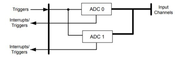
It has two identical successive Approximation Register (SAR) architecture based ADC modules such as ADC0 and ADC1 which share 12 analog input channels as shown in the figure below:
Each ADC input channel supports 12-bit conversion resolution. Furthermore, it has a built-in temperature sensor and a programmable sequencer to sample multiple input analog sources. The following table shows the GPIO pins which are used for alternate functions with analog input channels.
| Analog Chnnel | Pin Name | Pin Number |
|---|---|---|
| AN0 | PE3 | 6 |
| AN1 | PE2 | 7 |
| AN2 | PE1 | 8 |
| AN3 | PE0 | 9 |
| AN4 | PD3 | 64 |
| AN5 | PD2 | 63 |
| AN6 | PD1 | 62 |
| AN7 | PD0 | 61 |
| AN8 | PE5 | 60 |
| AN9 | PE4 | 59 |
| AN10 | PB4 | 58 |
| AN11 | PB5 | 57 |
ADC Resolution
12-bit resolution means the ADC converts the analog values between 0 to 3.3 volts into discrete digital values in the range of 0 to (2^12) – 1 or 0 to 4095. That means, if digital value is 0, the analog input to ADC channel is zero and if digital value is 4095, the analog input to ADC channel is 3.3 volts. This formula is used to calculate the minimum analog voltage ADC can measure:
Resolution = 3.3 volts / 4095 = 0.8mV
Here 0.8mV means the discrete digital value after conversion shows the 0.8 millivolts. For example, if the digital value measured by ADC is 2048, we can calculate analog voltage by multiplying digital value with 0.8 millivolts.
Analog voltage = 2048 x 0.8 = 1.65V
In short, the maximum voltage ADC can measure directly is 3.3 volts and the minimum is zero volts.
Note: We can measure higher voltages such as high DC voltage, AC voltage also. But we have to use a signal conditioning circuit. You can read these tutorials:
Sample Sequencers
As we mentioned earlier, TM4C123 microcontroller has two ADC modules that are ADC0 and ADC1. Each analog to digital converter has a separate sample sequencer (SS0, SS1, SS2 and SS3) which can sample different input channels. All these sequencers offer different numbers of samples that they can capture and the length of FIFO. The following table shows the number of samples and the length of FIFO for each sequencer circuit.
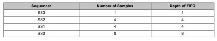
TM4C123GH6PM microcontroller supports sampling rate from 125 KSPS to 1 MSPS.
TM4C123G ADC Configuration and Initialization steps
In this section, we will discuss the different registers that are used to configure ADC input channels and sample sequencers of TM4C123 Tiva C Launchpad.
Followings are the steps to enable ADC module of TM4C123 Tiva C Launchpad:
Enable Clock to ADC
First, we enable the clock to ADC module and to the GPIO pin which is used as an analog input. RCGCADC register is used to enable the clock to ADC0 and ADC1 modules. Bit0 of RCGCADC enables ADC0 and bit1 of RCGCADC register enables ADC1. Setting the corresponding bit enables and clearing disables the clock to the corresponding analog to digital converter.
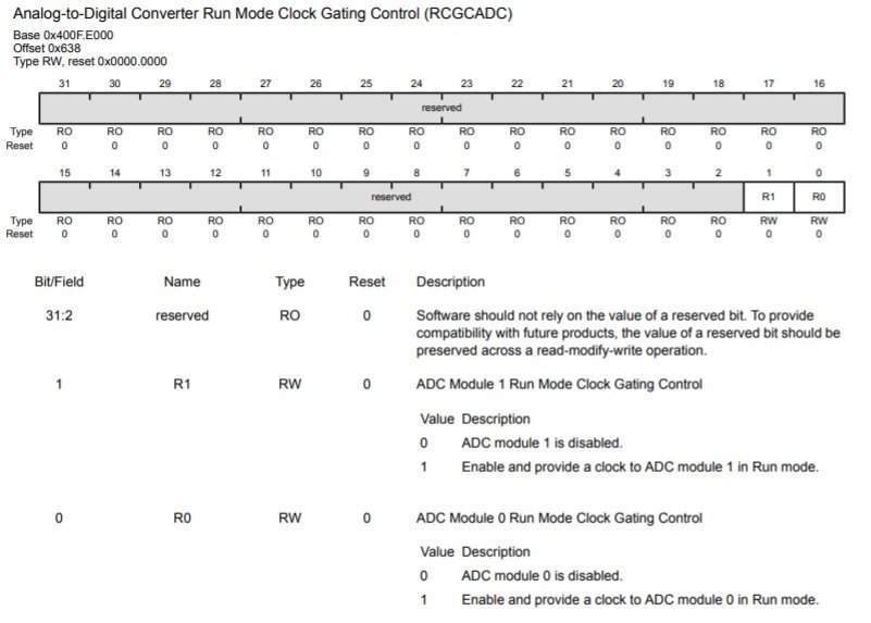
For example, we want to use ADC0, this line will enable clock to ADC0:
SYSCTL->RCGCADC |= (1UL<<0);RCGCGPIO register is used to enable clock to the related GPIO port pin which will be used to measure analog input. For example, we are using analog channel zero or AN0. As we mentioned earlier, AN0 takes analog signals from the PE3 pin of PORTE. Setting the 5th bit of RCGCGPIO register enables the clock to PORTE of TM4C123 microcontroller.
SYSCTL->RCGCGPIO |= (1UL<<5); Configure PORT as an Analog Pin
The next step is to configure the analog channel corresponding GPIO pin as an analog pin. To enable alternate function of PE3 pin as an analog input, three registers are used.
- AFSEL: This register selects alternate functions of each GPIO pin. Because each pin is multiplexed with different peripherals. This line enables the alternate function of PORTE pin 3 or PE3.
GPIOE->AFSEL |= (1UL<<3);- DEN : This register enables or disables the digital functionality of the corresponding GPIO port. This line disables the digital functionality of PE3 pin.
GPIOE->DEN &= ~(1UL<<3);- AMSEL: This register is used to enable analog function of GPIO pins. We are using PE3 pin for AN0.Therefore, we must enable PE3 analog function by setting the 3rd bit of AMSEL register.
GPIOE->AMSEL |= (1UL<<3);Sample Sequencer Configuration
As we mentioned earlier, the sample sequencer is part of ADC modules of TM4C123 microcontroller. It is used to get ADC samples and stores the conversion results in FIFO.
Activate ADC SS
ADCACTSS (active sample sequencer) register is used to enable or disable sample sequences SS0, SS1, SS2 and SS3. For example, we will be using SS3 in this tutorial. Setting ASEN3 bit of ADCACTSS register enables the SS3 and clearing it disables the SS3. Before configuring ADC channel, we must disable the sample sequencer by clearing bit3 like this:
ADC0->ACTSS &= ~(1UL<<3);Sampling Option
ADCEMUX register selects the trigger option to start sampling of an input signal for each sample sequencer. Trigger event sources are processor, PWM, analog comparators, external interrupts, and software. The default trigger option is by software. This line selects a software event as a start conversion trigger.
ADC0->EMUX &= ~0xF000;Analog Channel Selection
TM4C123G microcontroller provides 12 analog channels. ADCSSMUXn registers ( where n=0, 1,2,3 ) select analog channels for sample sequencers. For example, if we want to use SS3 and analog channel A0, this line will select AN0 analog channel for sample sequencer 3 or SS3.
ADC0->SSMUX3 = 0;ADC Sampling Rate Setting
ADCPC register is used to set the sampling rate of ADC. The Analog to digital converter module of the TM4C123G microcontroller supports a sampling rate from 125 KSPS to 1 MSPS. First four bits of the ADCPC register are used to set the sampling rate. This line sets the sampling rate to 250ksps.
ADC0->PC = 0x3;After ADC initialization and configuration, set the SS3 bit of ADCPSSI register to start ADC conversion for sample sequencer 3.
ADC0->PSSI |= (1UL<<3);If you are using ADC1 or other sample sequencers, select the corresponding bit of ADCPSSI register.
ADCRIS register provides raw interrupt signal for each sample sequencer on sample conversion completion. INR3 bit of ADCRIS register raw interrupt status of SS3. If you are using a polling method to get ADC value, you can keep polling this bit and read the data whenever the INR3 bit becomes one.
ADCSSFIFO0,ADCSSFIFO1, ADCSSFIFO2 and ADCSSFIFO3 registers contain the conversion result of ADC sample sequencers for SS0, SS1, SS2 and SS3 respectively. 12 least significant bits of these registers store conversion results.
How to use TM4C123G Tiva Launchpad ADC
In this section, we will see a demo code of TM4C123G microcontroller ADC. In this code, we configure and initialize the AN0 channel with the ADC0 module, and sample sequencer 3 is used to take input signal samples.
Schematic Diagram
We are using Analog channel zero or AN0 which takes input from PE3 pin. PE3 is a pin number three of PORTE of TM4C123 microcontroller.
In this schematic diagram, we are using a variable resistor to provide variable voltage input signal to AN0. Connect the middle terminal of a potentiometer with PE3/AN0 and other two terminals with 3.3 volts and ground terminal respectively.

ADC Code TM4C123G
This ADC code of TM4C123GH6PM microcontroller reads analog input from AN0 pin and based on digital value turns on or turns off the onboard green LED of TM4C123G Tiva C launchpad. If measured digital value is less than 2048 LED will remain off. If ADC digital value is greater than or equal to 2048, LED turns on.
/* TM4C123G Tiva C Series ADC Example */

/* This Program controls the onboard green LED based on discrete digital value of ADC */
/* If AN0 channel value is less 2048 digital value than LED turns off and otherwise remain on */
#include "TM4C123GH6PM.h"

int main(void)
{
     unsigned int adc_value;

    /* Enable Clock to ADC0 and GPIO pins*/
    SYSCTL->RCGCGPIO |= (1<<4);   /* Enable Clock to GPIOE or PE3/AN0 */
    SYSCTL->RCGCADC |= (1<<0);    /* AD0 clock enable*/

    /* initialize PE3 for AIN0 input  */
    GPIOE->AFSEL |= (1<<3);       /* enable alternate function */
    GPIOE->DEN &= ~(1<<3);        /* disable digital function */
    GPIOE->AMSEL |= (1<<3);       /* enable analog function */

    /* initialize sample sequencer3 */
    ADC0->ACTSS &= ~(1<<3);        /* disable SS3 during configuration */
    ADC0->EMUX &= ~0xF000;    /* software trigger conversion */
    ADC0->SSMUX3 = 0;         /* get input from channel 0 */
    ADC0->SSCTL3 |= (1<<1)|(1<<2);        /* take one sample at a time, set flag at 1st sample */
    ADC0->ACTSS |= (1<<3);         /* enable ADC0 sequencer 3 */

	  /*Iniitialize PF3 as a digital output pin */

   SYSCTL->RCGCGPIO |= 0x20; // turn on bus clock for GPIOF
   GPIOF->DIR       |= 0x08; //set GREEN pin as a digital output pin
   GPIOF->DEN       |= 0x08;  // Enable PF3 pin as a digital pin
    while(1)
    {
        ADC0->PSSI |= (1<<3);        /* Enable SS3 conversion or start sampling data from AN0 */
        while((ADC0->RIS & 8) == 0) ;   /* Wait untill sample conversion completed*/
        adc_value = ADC0->SSFIFO3; /* read adc coversion result from SS3 FIFO*/
        ADC0->ISC = 8;          /* clear coversion clear flag bit*/
			/*control Green PF3->LED */
			if(adc_value >= 2048)
	GPIOF->DATA  = 0x08; /* turn on green LED*/
	else if(adc_value < 2048)
	GPIOF->DATA  = 0x00; /* turn off green LED*/
    }
}

void SystemInit(void)
{
    SCB->CPACR |= 0x00f00000;
}
Now create a new project in Keil uvision IDE and upload this ADC code to TM4C123G Tiva Launchpad. If you don’t know how to use Keil IDE, check this article:
Rotate potentiometer to change the input signal value. You will notice that the green LED of TM4C123G Tiva Launchpad turns on when the digital value crosses 2047.
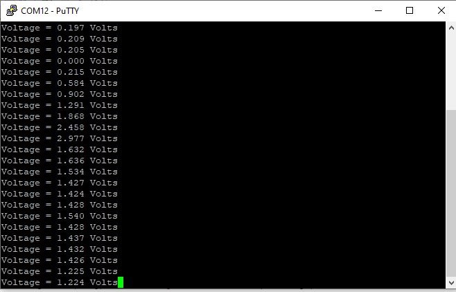
Measure Analog voltage with TM4C123G ADC
In the last section, we have seen an example to use ADC0 of TM4C123G microcontroller. We controlled an LED based on the digital value of the analog channel. In this section, we will see how to convert the measured discrete digital value back into voltage. For demonstration purposes, we will use the UART module TM4C123 microcontroller and send measured voltage value to the PC using USB to serial converter.
Circuit Diagram

If you don’t know how to use UART module of TM4C123 Tiva Launchpad, you can read these tutorials:
Analog Voltage Measurement Code
This code is similar to the code that we used in the last analog to digital converter example. The only difference is the conversion of digital value into analog voltage.
/* TM4C123G Tiva C Series ADC Example */

/* This Program measures analog voltage from analog Channel zero */
/* Also sends measured voltage value to computer virtual terminal using UART */
#include "TM4C123GH6PM.h"
#include <stdio.h>
void Delay(unsigned long counter);
void UART5_init(void);
void UART5_Transmitter(unsigned char data);
void printstring(char *str);
char mesg[12];
float voltage;
int main(void)
{
     unsigned int adc_value;
	   UART5_init();
    /* Enable Clock to ADC0 and GPIO pins*/
    SYSCTL->RCGCGPIO |= (1<<4);   /* Enable Clock to GPIOE or PE3/AN0 */
    SYSCTL->RCGCADC |= (1<<0);    /* AD0 clock enable*/

    /* initialize PE3 for AIN0 input  */
    GPIOE->AFSEL |= (1<<3);       /* enable alternate function */
    GPIOE->DEN &= ~(1<<3);        /* disable digital function */
    GPIOE->AMSEL |= (1<<3);       /* enable analog function */

    /* initialize sample sequencer3 */
    ADC0->ACTSS &= ~(1<<3);        /* disable SS3 during configuration */
    ADC0->EMUX &= ~0xF000;    /* software trigger conversion */
    ADC0->SSMUX3 = 0;         /* get input from channel 0 */
    ADC0->SSCTL3 |= (1<<1)|(1<<2);        /* take one sample at a time, set flag at 1st sample */
    ADC0->ACTSS |= (1<<3);         /* enable ADC0 sequencer 3 */


    while(1)
    {
        ADC0->PSSI |= (1<<3);        /* Enable SS3 conversion or start sampling data from AN0 */
        while((ADC0->RIS & 8) == 0) ;   /* Wait untill sample conversion completed*/
        adc_value = ADC0->SSFIFO3; /* read adc coversion result from SS3 FIFO*/
        ADC0->ISC = 8;          /* clear coversion clear flag bit*/

			  /* convert digital value back into voltage */
			 voltage = (adc_value * 0.0008);
			sprintf(mesg, "\r\nVoltage = %0.3f Volts", voltage);
			 printstring(mesg);
      Delay(2000);
    }
}

void UART5_init(void)
{
	SYSCTL->RCGCUART |= 0x20;  /* enable clock to UART5 */
    SYSCTL->RCGCGPIO |= 0x10;  /* enable clock to PORTE for PE4/Rx and RE5/Tx */
    Delay(1);
    /* UART0 initialization */
    UART5->CTL = 0;         /* UART5 module disbable */
    UART5->IBRD = 104;      /* for 9600 baud rate, integer = 104 */
    UART5->FBRD = 11;       /* for 9600 baud rate, fractional = 11*/
    UART5->CC = 0;          /*select system clock*/
    UART5->LCRH = 0x60;     /* data lenght 8-bit, not parity bit, no FIFO */
    UART5->CTL = 0x301;     /* Enable UART5 module, Rx and Tx */

    /* UART5 TX5 and RX5 use PE4 and PE5. Configure them digital and enable alternate function */
    GPIOE->DEN = 0x30;      /* set PE4 and PE5 as digital */
    GPIOE->AFSEL = 0x30;    /* Use PE4,PE5 alternate function */
    GPIOE->AMSEL = 0;    /* Turn off analg function*/
    GPIOE->PCTL = 0x00110000;     /* configure PE4 and PE5 for UART */
}
void UART5_Transmitter(unsigned char data)
{
    while((UART5->FR & (1<<5)) != 0); /* wait until Tx buffer not full */
    UART5->DR = data;                  /* before giving it another byte */
}

void printstring(char *str)
{
  while(*str)
	{
		UART5_Transmitter(*(str++));
	}
}
void Delay(unsigned long counter)
{
	unsigned long i = 0;

	for(i=0; i< counter*1000; i++);
}
void SystemInit(void)
{
    SCB->CPACR |= 0x00f00000;
}
As we mentioned earlier, each analog channel is of 12-bit resolution.That means each step of ADC digital value is of 0.8 millivolts. Therefore, if we want to convert measured digital value into analog voltage, we multiply ADC output value with resolution like this:
Analog voltage = Measured Digital Value x 0.8 millivolts
Hence, by using the above formula, this line converts ADC digital value into analog voltage.
voltage = (adc_value * 0.0008);After that we use a previously developed UART function to transmit measured voltage values to personal computers.
Enable TM4C123G ADC Interrupt
In the last two examples, we used a polling method to measure analog signal value with TM4C123 microcontroller ADC. But the polling method is not an efficient method and it’s a wastage of microcontroller processing time and resources. Instead of using a polling method where we keep polling for ADC conversion to complete using bit3 of ADCRIS register, we can use the ADC interrupt handler function to read the ADC conversion value.
As we have seen inn last two example, we keep polling for ADC conversion to complete using this line:
while((ADC0->RIS & 8);TM4C123 microcontroller keeps executing this loop and will not perform any useful function until ADC conversion is not completed. Hence, to avoid this wastage of microcontroller processing time, we can enable ADC data reception using ADC0 handler function.
Enable TM4C123 ADC Interrupt Mask
In order to enable ADC0 interrupt, ADC Interrupt Mask (ADCIM) is used. Setting bit3 of the ADCIM register enables the SS3 Interrupt Mask.
As you know that in ARM Cortex-M4 microcontroller, NVIC or nested vectored interrupt controller manages all interrupts. TM4C123 microcontroller supports 78 peripheral interrupts which are also known as IRQs. Before using each peripheral interrupt handler, we should enable each peripheral interrupt request to each NVIC using NVIC interrupt control register. The interrupt number of ADC0SS3_IRQn is 17. This line enables ADC0 sequencer 3 interrupt in NVIC.
NVIC->ISER[0] |= 0x00010001; /* enable IRQ17 for ADC0SS3*/Exception numbers are defined inside the header file of TM4C123GH6PM microcontroller and interrupt vector table.
The next step is to find the name of the interrupt handler function of ADC0SS3_IRQn inside the startup file of TM4C123G microcontroller. If you check startup file, you will find its name as shown in figure below:
ADC0Seq3_Handler ()Now receive data from the FIFO register of SS3 inside this function. This ADC0Seq3_Handler () function will execute whenever interrupt occurs due to sample sequencer 3.
TM4C123G ADC Interrupt Code
/* TM4C123G Tiva C Series ADC Example */

/* This Program measures analog voltage by using ADC0 via interrupt method*/
/* TM4C123G ADC Interrupt Example */
#include "TM4C123GH6PM.h"
#include <stdio.h>
void Delay(unsigned long counter);
void UART5_init(void);
void UART5_Transmitter(unsigned char data);
void printstring(char *str);
char mesg[12];
volatile float voltage;
volatile unsigned int adc_value;
void ADC0SS3_Handler(void){


	adc_value = ADC0->SSFIFO3; /* read adc coversion result from SS3 FIFO*/
	ADC0->ISC = 8;          /* clear coversion clear flag bit*/
  ADC0->PSSI |= (1<<3);        /* Enable SS3 conversion or start sampling data from AN0 */

}


int main(void)
{
	   UART5_init();
    /* Enable Clock to ADC0 and GPIO pins*/
    SYSCTL->RCGCGPIO |= (1<<4);   /* Enable Clock to GPIOE or PE3/AN0 */
    SYSCTL->RCGCADC |= (1<<0);    /* AD0 clock enable*/

    /* initialize PE3 for \AIN0 input  */
    GPIOE->AFSEL |= (1<<3);       /* enable alternate function */
    GPIOE->DEN &= ~(1<<3);        /* disable digital function */
    GPIOE->AMSEL |= (1<<3);       /* enable analog function */

    /* initialize sample sequencer3 */
    ADC0->ACTSS &= ~(1<<3);        /* disable SS3 during configuration */
    ADC0->EMUX &= ~0xF000;    /* software trigger conversion */
    ADC0->SSMUX3 = 0;         /* get input from channel 0 */
    ADC0->SSCTL3 |= (1<<1)|(1<<2);        /* take one sample at a time, set flag at 1st sample */

	  /* Enable ADC Interrupt */
	ADC0->IM |= (1<<3); /* Unmask ADC0 sequence 3 interrupt*/
	NVIC->ISER[0] |= 0x00020000; /* enable IRQ17 for ADC0SS3*/
  ADC0->ACTSS |= (1<<3);         /* enable ADC0 sequencer 3 */
	ADC0->PSSI |= (1<<3);        /* Enable SS3 conversion or start sampling data from AN0 */


    while(1)
    {

			  /* convert digital value back into voltage */
			 voltage = (adc_value * 0.0008);
			 sprintf(mesg, "\r\nVoltage = %0.3f Volts", voltage);
			 printstring(mesg);
      Delay(2000);
    }
}


void UART5_init(void)
{
	SYSCTL->RCGCUART |= 0x20;  /* enable clock to UART5 */
    SYSCTL->RCGCGPIO |= 0x10;  /* enable clock to PORTE for PE4/Rx and RE5/Tx */
    Delay(1);
    /* UART0 initialization */
    UART5->CTL = 0;         /* UART5 module disbable */
    UART5->IBRD = 104;      /* for 9600 baud rate, integer = 104 */
    UART5->FBRD = 11;       /* for 9600 baud rate, fractional = 11*/
    UART5->CC = 0;          /*select system clock*/
    UART5->LCRH = 0x60;     /* data lenght 8-bit, not parity bit, no FIFO */
    UART5->CTL = 0x301;     /* Enable UART5 module, Rx and Tx */

    /* UART5 TX5 and RX5 use PE4 and PE5. Configure them digital and enable alternate function */
    GPIOE->DEN = 0x30;      /* set PE4 and PE5 as digital */
    GPIOE->AFSEL = 0x30;    /* Use PE4,PE5 alternate function */
    GPIOE->AMSEL = 0;    /* Turn off analg function*/
    GPIOE->PCTL = 0x00110000;     /* configure PE4 and PE5 for UART */
}
void UART5_Transmitter(unsigned char data)
{
    while((UART5->FR & (1<<5)) != 0); /* wait until Tx buffer not full */
    UART5->DR = data;                  /* before giving it another byte */
}

void printstring(char *str)
{
  while(*str)
	{
		UART5_Transmitter(*(str++));
	}
}
void Delay(unsigned long counter)
{
	unsigned long i = 0;

	for(i=0; i< counter*1000; i++);
}
void SystemInit(void)
{
    SCB->CPACR |= 0x00f00000;
}
Keil uvision v5 Instructions
Note: If you are using Keil uvision v5, you should remove the void SystemInit(void) function from the above code. Because the startup file in Keil v5 already contains the function SystemInit().
After that follow these steps to build above code with Keil uvision 5:
The other issue with the SystemInit() function in the new system_TM4C123.c is that it configures the clock generation which results in a different system clock rate than the default 16 MHz frequency. But the above sample code works on the default 16 MHz system clock. Therefore, the above program creates timing issues with Keil v5. You may retain the default system clock rate in Keil v5, by the following steps:
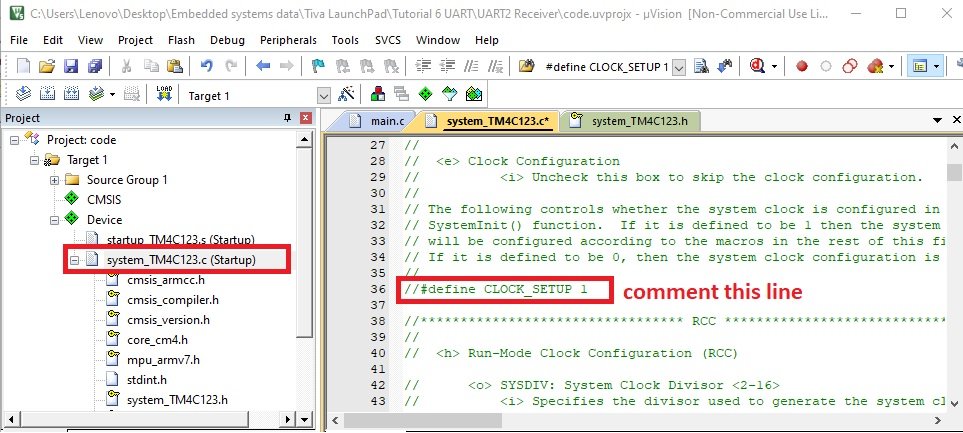
- Expand the Project->Device to show system_TM4C123.c (startup)
- Double click to open the file in the editor window
- Find the line “#define CLOCK_SETUP 1” as the figure below
- Comment out the line
- Rebuild the project
Related content:
- MPU6050 Gyroscope Accelerometer sensor interfacing with TM4C123G Tiva C Launchpad
- I2C Communication TM4C123G Tiva C Launchpad
- UART Communication TM4C123 Tiva C LaunchPad with Example Codes
- SPI Communication TM4C123 – Communication Between Tiva Launchpad and Arduino
- HC-SR04 Ultrasonic Sensor Interfacing with TM4C123 – Distance Measurement Example
Would you mind telling me how to use a different sequencer (0), and how to use multiple ADC inputs?
Copying and compiling the TM4C123G Tiva C Series ADC Example i get an error:
.\Objects\FirstLEDproj.axf: Error: L6200E: Symbol SystemInit multiply defined (by system_tm4c123.o and main.o).
Not enough information to list image symbols.
Not enough information to list load addresses in the image map.
Missing a precompilerdirective ? I can’t figure out what’s lacking.
Could you please help out ?
Maybe, you need to use an updated startup file. Can you share the more information on which image symbol name is missing. It must be showed on the error console log.
I’ll look into this and get back to you.
Hi, i am facing to same issue. Did you find any solution for this problem?
Hallo again.
First of all I would like to thank you for a fantastic site.
I am progressing with the other tutorials, but I got stuck with the ADC-examples.
I created a new project,
source group 1
main.c
cmsis_armcc.h
cmsis_compiler.h
cmsis_version.h
core_cm4.h
mpu_armv7.h
stdint.h
system_TM4C123.h
TM4C123.h
TM4C123GH6PM.h
CMSIS
Device
startup_TM4C123.s
system_TM4C123.c
Then I simply made a copy of your main.c so I will not reproduce it here.
When compiling I got this result.
Build started: Project: NewProj
*** Using Compiler ‘V5.06 update 7 (build 960)’, folder: ‘C:\Keil_v5\ARM\ARMCC\Bin’
Build target ‘Target 1’
compiling main.c…
linking…
.\Objects\NewProj.axf: Error: L6200E: Symbol SystemInit multiply defined (by system_tm4c123.o and main.o).
Not enough information to list image symbols.
Not enough information to list load addresses in the image map.
Finished: 2 information, 0 warning and 1 error messages.
“.\Objects\NewProj.axf” – 1 Error(s), 0 Warning(s).
Target not created.
Build Time Elapsed: 00:00:00
Hi, if you are using Keil uvision 5, remove this function SystemInit() from your code and compile code again.
You can also try with Keil uvision 4. Maybe this video demo helps you?