FIELD PROGRAMMABLE GATE ARRAY(FPGA): Now we look at the FPGA (Field Programmable Gate Arrays). This article is a introduction of field programmable gate array that is FPGA. Now the question is “What is an FPGA…?” FPGA is a programmable device, a programmable chip which actually allows you to design your own chip. It allows you to design and implement virtually any digital function you can imagine in one universal chip. I am going to write series of tutorials on FPGA modules using spartan 3 FPGA module. I will start tutorials on FPGA module soon. This is a first article on series on tutorials on field programmable gate arrays.
FPGAs are used to design higher level of complexity circuits like customized circuits using reconfigureable gate arrays or logic cells. In gate arrays we have manufacured designed rectengular cells which are in usually in usually two dimensional array topology. we have connecting wires between these cells which are used to connect these gate arrays with each other through a languages like verilog and VHDL. we can aslo customize each cell to become a combinational or sequential logic device like gates and flip flops. This is a fastest way to design ASIC chips without the need of ordering or manufacture them.
you may also like to check this:
Difference between FPGA and microcontrollers
The big difference between FPGA and virtually every of the chip -you can buy on the market- is that it has no intended function which you actually buy at the market all others chip can actually perform something or do something useful but an FPGA can’t even do that. They are completely stupid but they are extremely flexible and allows you to design anything you can imagine in the digital term and you can program it. Unlike a microcontroller, it is very flexible but FPGAs consumes more power than typical microcontroller. You can actually program it into digital programming chip If you want to turn an FPGA into an AVR Microcontroller or PIC microcontroller you can do that.
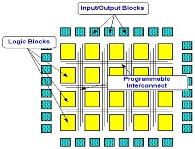
If you want to turn it digital signal processor, you can do that, and if you want to turn it into thousand LED custom driver you can do that, it is incredibly flexible only by your imagination. So how can I do this? I do it by containing thousands, 10 thousand, 100 thousand even more of individual logic elements let’s call them CLB (configurable logic block) that can implement pretty much in basic functions you can imagine, and you can configure them in any way you like to perform any complex or even simple digital function. These are configurable logic blocks setting aside these lines in the figure. These lines are middle interconnections you can join up in any configuration possible side you might join one logic block to next one and same like this you join all logic blocks.
Major FPGA vendors
Followings are the major FPGA vendors in market. They also provide easy to use FPGA development boards.
- Xilinx
- Altera Corp
- Atmel
- Lattice semi conductor
Field programmable gate array block diagram structure
All over the place to implement whatever the function you programmed into this thing. So they are often God like a safe Gates because they are just only configurable gates seeking on interconnecting logic and well that a bit of old term because here are configurable CLBs (configurable logic blocks) or logic elements are moving just individual gates there pretty smart on their own. Now, in theory, there are most helpful and flexible FPGAs or configurable logic chip would contain millions of main gates and an infinite network all these interconnect lines to join them all together because if you remember basic digital logic theory and main gate if you have enough main Gate, you can create anything, you can create a microcontroller even you can create a hundred microcontrollers and perform any function you can imagine or you like to do anything just from the main gate. Unfortunately, chips actually do exist well not much use anymore… So a modern FPGA is basically an optimization of more complex configurable logic blocks that do contains individual Gate and elements but also contain flip- flops, look up tables and things like that more complex blocking there then surrounded by a limited number of interconnect trice is like this as shown in above figure. And then a balance tide of between logic blocks.
CLB Configuration Logic Blocks of FPGA
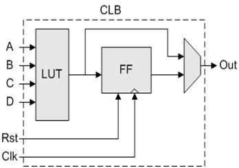
Let’s take an extremely brief look get what inside a CLB, this is very generic. In practice they are more complicated but generally what inside CLB, the basic input we can see, look up the table! There are four input (A,B,C,D). This can get larger one depending on FPGAs types and then we get allow configuration fuses in there. Actually you can perform a particular function in LUT. They typically have one or more flip- flops in here as well. You can use that flip – flops in various ways that are connected to dedicated block lines or you can come from the fabric and others more switching stuff up there. You might got a bunch of logic gates and some flip- flops and then we might get some output as well and you watch thousands things incredibly become powerful and flexible.
IOB of FPGA (Input/output blocks)
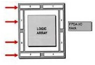
Now the other thing from joining side all the I/O blocks, around the CLBs that actually connect to the individual pins on the chip and these are very complicated blocks. They can perform all source of the function just like a micro program you can control them and you can have a different logic standard as well on the various pin that can contain flip – flops for designing PDR memory and all sorts of complicated things.
So you have got a lot of these logic blocks and you can combine them to perform various functions combine with pretty powerful arrays that can do any thing you imagine. FPGA has no ability to store their internal configuration and how you program the device as soon as the light turns off, it forgets what to do. If you want FPGA to be useful you can’t just have FPGA, you got some mandatory external configuration, flash memory which is basically a regular serial the flash memory device except that contains all of the information and all of these little fuses inside here. Which logic blocks connect to which block and how ? and the fuses inside here in CLB and IOB is what these I/O blocks stand.That’s why we need a larger external memory because of a lot of fuses inside here which have to be programmed. They are not just the fuses they are the transistors that do everything .. but when you turn on FPGA, everything has been gone.
Advantages of FPGA
So what are the advantages of FPGA? The main advantages are
- You can do everything, you can imagine.
- They are also super-fast and some of them, even the basic FPGA have I/O blocks. They are super-fast
- They can actually do gig bits if you can compare that micro even though a very modern processor, 100 MH2 . You can do series processes 100 MH2 but with FPGA it’s not a problem because you can dedicate a logic in here… and that will come down a massively parallel, very incredible from the speed point of view.
Now field programmable is differed than micro processor which can be reprogrammed because this met just a processor fixed, you can program it. You can just reconfigure it into whatever you want. They are powerful because they aren’t just the custom thing they can be changed to anything.
FPGA programming language
Two programming languages are usually used for programming of FPGA based development boards.
- Verilog
- HDLs : High level descriptive language. It is used to describe architecture and behavior of an electronics systems.
HDL has following advantages:
- Generic design
- Higher productivity level
- Easy understanding than schematics
- Architecture test at very early stage
- Design re usability
HDL has following disadvantages:
- No control for gate level
- Logic implementation are inefficient
- Synthesis not standard
disadvantages of FPGAs
The FPGA is so, much useful then why it is not at every home or in every product because there are a lot of disadvantages of FPGAs.
- Expensive
- Use high power
- Volatile
- High pin count
- Complicated
- Many traps
- Complex tools
- Hard to choose/ compare
- HDL not easy
Why FPGA’s are not common in every product?
FPGA is expensive because there are a lot of chips in them. There are a lot of parallel chips which can actually perform the same things. You can spend thousands of dollars to just have one FPGA. FPGA is some of the leading.Processor chip in market, because they contain million of logic gates, just to give you the flexibility. So because there are a lot of flexibility so they are not made for power optimization. So they are actually high power devices. They are volatile because they forget anything.
you have to program it anytime so it may get more bootable. If you are looking for a friendly device then FPGA is not a friendly device because of high pins. Go and download the function of CLB and IOB, their function find the rest of life to find low things actually works. There’s a lot traps in FPGA in term of configuring the CLB and IOB because some of I/O blocks have links to other that are so speed.There is a lot of tools in FPGA data complex that look easy but they are really complex. They are hard to choose and compare with another in the market. So,there are a lots of disadvantages in FPGA that’s why its not so common in every product.

