In this tutorial, we will explain how to initialize a GPIO (General-purpose input-output) pins of the TM4C123GH6PM microcontroller with the Tiva C series launchpad. In order to use the GPIO pin of a TM4C123G evaluation kit, we must first initialize the registers related to GPIO pins. At the end of the tutorial, the built-in LED of the TIVA board is blinked using the associated GPIO port with it.
The basic initialization includes:
- Initialization of the main clock of the board
- Enabling specific port registers of which the GPIO pins will be used
- Initialization of GPIO port pins to either digital output or digital input .i.e. setting the direction pins
- After that, the functionality of the port is selected if it is to be alternative or not (in this tutorial we are not using alternative functionality so skip it at this moment)
TM4C123GH6PM Microcontroller GPIO pins
TM4C123GH6PM belongs to the ARM Cortex M4 microcontroller series. It has six GPIO ports such as PORTA, PORTB, PORTC, PORTD, and PORTE. Each port has a different number of pins as given in this table.

| GPIO Ports | Pins |
|---|---|
| PORTA | PA0 – PA7 |
| PORTB | PB0- PB7 |
| PORTC | PC0 – PC7 |
| PORTD | PD0 – PD7 |
| PORTE | PE0 – PE5 |
| PORTF | PF0-PF7 |
All the address range of port A to port F are given in the table below. As you can see from this table, a total of 4K bytes of memory is allocated for each PORT. The reseason for this larger amount of memory for each port is due to many functions and special functions registers associated with each port of TM4C123G.
| Port name | Starting address | Ending address |
| PortA | 0x40004000 | 0x40004FFF |
| PortB | 0x40005000 | 0x40005FFF |
| PortC | 0x40006000 | 0x40006FFF |
| PortD | 0x40007000 | 0x40007FFF |
| PortE | 0x40024000 | 0x40024FFF |
| PortF | 0x40025000 | 0x40025FFF |
The initialization steps that are required to configure the TM4C123GH6PM microcontroller pins as GPIO pins are discussed here.
For some GPIO pins, a few additional steps might be required. For instance, some of the GPIO pins are assigned special functionality by default, and to configure them as general-purpose input-output pins, we need to unlock or unmask the pin. It is possible to configure a GPIO pin as an alternative functionality multiplexing, which will be explained in upcoming tutorials. Basic steps for TM4C123GH6PM launchpad configuration as a GPIO are listed below,
- Clock configuration
- Data control configuration
- Mode control configuration
- Pad control configuration
Each configuration step requires enabling or disabling a bit field in one or more registers. Writing a specific value in an appropriate register effectively means the configuration of a pin on microcontroller. I will explain each of them in detail shortly.
GPIO Pins Clock Enable Register
The first step in GPIO configuration is to enable the clock for a particular peripheral you want to enable. A particular port can be enabled by setting an appropriate bit field for the required GPIO port in the RCGCGPIO register.
The name of the GPIO clock register is a very important entity here. These register names are defined using physical addresses that belongs to GPIO pins. These names must not be changed and all peripheral register names are specified using pointers and structures and you can take a look by going inside the header file of a microcontroller on this location:
C:\Keil\ARM\INC\TI\TM4C123\TM4C123GH6PM.h
Instead of initializing everything from the physical addresses, we can use header files of a microcontroller which comes with the installation of Keil IDE. Therefore, the best way is to use them as it is.
RCGCGPIO register is mapped to the address 0x400FE608. All these memory address mappings are provided in the datasheet of TM4C123GH6PM microcontroller. The bit 0 to bit 5 of RCGC_GPIO_R register are used to enable the port A to port F on the peripherals respectively.
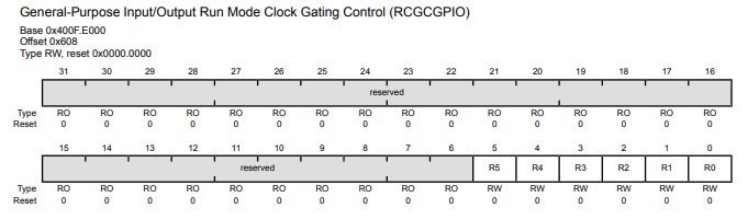
For instance, if we enable the enable clock for port C, we set the 2nd bit of the RCGCGPIO register and similarly for other ports.
RCGCGPIO |= 0x01 //Enable clock for PORTA
RCGCGPIO |= 0x02 //Enable clock for PORTB
RCGCGPIO |= 0x04 //Enable clock for PORTC
RCGCGPIO |= 0x08 //Enable clock for PORTD
RCGCGPIO |= 0x01 //Enable clock for PORTE
RCGCGPIO |= 0x02 //Enable clock for PORTF
TM4C123G GPIODATA Register
The GPIO port pins of TM4C123G are multiplexed with different peripherals such as digital I/O, PWM, serial communication, etc. But each pin can be used for only one functionality at a time. GPIODEN register is used to enable GPIO pins as digital input-output pins.
When the port pin is configured as GPIO pins, the GPIODATA register is used to read and write data on the registers. If the pin is configured as a digital output pin, the data written to the GPIODATA register reflects on the corresponding output pin.
Bit Branding
This allows us to read or write data from individual GPIO pins in a single instruction cycle without actually affecting the present state of other GPIO pins. This is the basic definition of data masking in microcontrollers. In the address bus, the bit number [9:2] is used to construct the mask. A total of 256 bits of addresses are allocated to the data register. According to the value given in the address of the GPIO_DATA_R register, the corresponding bit will be enabled and the data register will read data only from that specified port and will not check the data on remaining ports.
For instance, if we specify an address of 0x400253FC to the data register of port F the last [9:2] bits of the address register will be set i.e. the value of last bits will be 1111111100 where the last two zero bits are not in use. This will enable all the pins present on the port F of TIVA peripherals. If we are interested in enabling pin 1 only then the address given to the data register will be 0x40025000+0x008; which corresponds to the base address of PORTF and offset address of PORTFDATA register.
TM4C123G GPIODIR Direction Control Register
The third configuration step is the direction control configuration. You might be wondering what does direction control represents. A GPIODIR register decides, which pins of the PORT will be configured either as a digital input or a digital output. The individual configuration capability of each GPIO is applicable to other registers of the GPIO port pins.
If we want to enable a pin of a port as digital input-output the corresponding bit on the GPIODIR register should be set or reset. If we want to configure a particular pin of any port as a digital input pin, the corresponding e data direction bit should be cleared. Similarly, if we want to configure a particular pin of any port as a digital output pin, the corresponding data direction bit should be set to one.
Note: All pins are by default configured as a digital input.
LED Blinking Example TM4C123G Tiva LaunchPad
Let’s do a simple example of blinking the built-in LEDs of the TIVA C Series Launchpad. Using the steps mentioned above, we will now write the TM4C123G code that will blink the LED present on the board.
We will be using Keil Uvision to write a program for TM4C123G launchpad. If you don’t know how to use Keil IDE, check these tutorials:
First of all, create a blank project as discussed in the previous tutorial or use the project you created previously. The main page of the project is shown in the figure below. Don’t forget to make all the necessary changes discussed in the previous tutorial.
Registers Defintion File
Pointer variables are used to interact with memory directly. Register definition file provides a list of peripheral register along with their descriptive names. This register definition files provide a list of peripheral registers address that maps to their user-friendly name. Now let’s see how to create a register definition file for this example. But, all microcontroller manufacturers also provide register files in their IDE, so we do not need to create a registers definition file. This method is called directly dereferencing memory using pointers.
In GPIO configuration first method is to enable the clock of the peripherals. We will first define macros of all the registers containing the address of the required pin needed for configuration and after that, we will assign them the values in the main code.
Enable Clock Example
To enable the clock for PORTF, first, we need to define the physical address of the RCGCGPIO register. According to the datasheet, the base address of RCGCGPIO is 0x400FE000, and the offset address is 0x608. Hence,
Physical address of RCGCGPIO = 0x400FE000+0x608=0x400FE608Define a macro name “SYSCTL_RCGCGPIO_R” which is a pointer to the address of clock enable register. This line defines the address of the RCGCGPIO register using preprocessor macro and addresses dereferencing directly with pointers.
# define SYSCTL_RCGCGPIO_R (*(( volatile unsigned long *)0x400FE608))
Configure PORTF as a digital PORT
After clock enabling, the next step is to configure the PORTF as a digital output. Because Tiva launchpad built-in LEDs are present on pin1 pin2 and pin3 of port F.
The address range of port F is from 0x4002500-0x40025FFF. But the question is where the values assigned to the data register GPIODATA of PORTF?? As we want to enable pins 1-3 of port F. First, we need to find the physical address of GPIODEN register for PORTF. For that, we need to know the base address of PORTF and offset- address of GPIODEN register. According to the datasheet of TM4C123GH6PM microcontroller,
GPIO PORTF base address = 0x4002 5000
GPIODEN Register offset address = 0x51c // page number 682 TM4C123GH6PM datasheet
physical address = 0x40025000+0x51C = 0x4002551C
This line defines a macro to the physical address of GPIODEN register.
# define GPIO_PORTF_DEN_R (*(( volatile unsigned long *)0x4002551C)) Setting PORTF Direction
The next step is to configure the direction register of PORTF. First, we need to define the physical address of the direction control register GPIODIR of PORTF. According to the datasheet,
Base address of PORTF = 0x40025000
Offset address of GPIODIR = 0x400 // // page number 663 TM4C123GH6PM datasheet
GPIODIR Physical address =  0x40025000+0x400 = 0x40025400
Define a macro name it properly and assign it a value of 0x40025400 which is the address allocated to direction register in memory as shown below:
# define GPIO_PORTF_DIR_R *(( volatile unsigned long *)0x40025400)) POTF GPIODATA Register
The physical address of the GPIODATA register of PORTF. According to the datasheet,
PORTF Base Address  =   0x40025000
GPIODATA Registe offset address = is 0x000
GPIODATA  Physical address = 0x40025000+0x608 = 0x40025000
As we want to enable pin1, 2, and 3 of PORTF. Hence, the binary bits that should be given to the data register are 000011100 whose equivalent hexadecimal number is 0x38 thus the address will be 0x4002500+0x38 which will be 0x40025038.
#define GPIO_PORTF_DATA_R (*(( volatile unsigned long *)0x40025038))
Turn on onboard LEDs of Tiva LaunchPad
Now let’s combine the above-given code and control onboard LEDs of tiva launchpad. Three LEDs are connected with PORTF pins 1, 2, and 3.
- PF1 – LED red
- PF2 – LED blue
- PF3 – LED green
This code turns on red LED which is connected with PF1 pin of PORTF.
#define SYSCTL_RCGCGPIO_R (*(( volatile unsigned long *)0x400FE608 ) )
#define GPIO_PORTF_DATA_R (*(( volatile unsigned long *)0x40025038 ) )
#define GPIO_PORTF_DIR_R  (*(( volatile unsigned long *)0x40025400 ) )
#define GPIO_PORTF_DEN_R  (*(( volatile unsigned long *)0x4002551C ) )


int main ( void )
{
SYSCTL_RCGCGPIO_R |= 0x20; // Enable clock for PORTF
GPIO_PORTF_DEN_R  = 0x0E;  // Enable PORTF Pin1, 2 and 3 as a digital pins
GPIO_PORTF_DIR_R  = 0x0E;  // Configure ORTF Pin1, 2 and 3 digital output pins

	while (1)
		{
		GPIO_PORTF_DATA_R |= 0x02; // turn on red LED
		}
}
Above code is self explainatory except the line given below. It sets the pin 1 of tiva c launchpad to one. Hence, it turns on red LED.
GPIO_PORTF_DATA_R |= 0x02; // turn on red LEDSimilary, we can control other two LEDs also.
GPIO_PORTF_DATA_R |= 0x04; // turn on blue LED
GPIO_PORTF_DATA_R |= 0x08; // turn on green LED
Now instead of defining your own register definition file, we can use header file available in compiler. As you can see, the code becomes pretty simple and short.
#include "TM4C123.h" // header files contains memory addresses listing
int main ( void )
{
SYSCTL->RCGCGPIO|= 0x20;
GPIOF->DIR = 0x02;
GPIOF->DEN = 0x02;

	while (1){
	GPIOF->DATA = 0x02; // turn on red LED

    }
}
Video Demo
Blinking LED Example TM4C123G LaunchPad
In this section, we will see how to contol or blink these LEDs with some delay.
Assign values to Registers
The pin 1 enable button to have a value of 0x20 (10) because it will set the second bit of the enable register similarly 0x04 (100) for pin 2 will set the 3rd pin of the digital to enable to register and 0x08 (1000) will set the 4th pin of the enable register. Similarly LED_ON1, LED_ON2, and LED_ON3 will set the 2nd 3rd and 4th bits of the data register respectively. This will be done in the main code.
# define GPIO_PORTF_CLK_EN	 0x20
# define GPIO_PORTF_PIN1_EN	 0x02
# define LED_ON1 	         0x02
# define GPIO_PORTF_PIN2_EN    	 0x04
# define LED_ON2		 0x04
# define GPIO_PORTF_PIN3_EN	 0x08
# define LED_ON3 		 0x08
Now write a delay function that will be used to cause a delay between the blinking of two different LEDs otherwise they will merge the colors.
#define DELAY_VALUE 1000000
unsigned long j=0;
void Delay(void){
	for (j=0; j<DELAY_VALUE ; j++);
}
LED Blinking main code
Now lets’ move to the main code of the program. In the main code we will first assign the value of the cock to the register to which we specified the clock address as shown in the figure below,
The “|=” operator is an OR operator and it will simply add the value at the right to the variable given at the left. The uloop variable and the statement containing uloop is present there only to halt 3 clock cycles before moving to peripherals, which is a must while working with TIVA. Now move to the enabling of DIR and DEN registers. Simply OR the macros containing the values of the enable and direction registers with the macros containing the address of the registers as shown in the figure below,
GPIO_PORTF_DIR_R |= GPIO_PORTF_PIN1_EN ;
GPIO_PORTF_DEN_R |= GPIO_PORTF_PIN1_EN ;
GPIO_PORTF_DIR_R |= GPIO_PORTF_PIN2_EN ;
GPIO_PORTF_DEN_R |= GPIO_PORTF_PIN2_EN ;
GPIO_PORTF_DIR_R |= GPIO_PORTF_PIN3_EN ;
GPIO_PORTF_DEN_R |= GPIO_PORTF_PIN3_EN ;
Now, if we want to turn ON the LED we will OR the macro containing the value with the macro containing the data register address and if we want to turn OFF the LED we will AND the macro containing the value with the macro containing the data register address. We will turn the LEDs ON and OFF with delays in between to blink the LEDs as shown in the figure below,
while (1)
	{
	GPIO_PORTF_DATA_R &= LED_ON3;
	GPIO_PORTF_DATA_R &= LED_ON2;
	GPIO_PORTF_DATA_R |= LED_ON1;
	Delay();
	GPIO_PORTF_DATA_R &= LED_ON1;
	GPIO_PORTF_DATA_R &= LED_ON2;
	GPIO_PORTF_DATA_R |= LED_ON3;
	Delay();
	GPIO_PORTF_DATA_R &= LED_ON3;
	GPIO_PORTF_DATA_R &= LED_ON1;
	GPIO_PORTF_DATA_R |= LED_ON2;
	Delay();
	}
Now connect the TIVA Launchpad with your laptop and build the code using the built button and then load it using the load icon as shown in the figure below. This will load your code on the microcontroller and the LEDs will start blinking

Complete Code LED Blinking Tiva LaunchPad
#define SYSCTL_RCGCGPIO_R (*(( volatile unsigned long *)0x400FE608 ) )
#define GPIO_PORTF_DATA_R (*(( volatile unsigned long *)0x40025038 ) )
#define GPIO_PORTF_DIR_R  (*(( volatile unsigned long *)0x40025400 ) )
#define GPIO_PORTF_DEN_R  (*(( volatile unsigned long *)0x4002551C ) )

#define GPIO_PORTF_CLK_EN  0x20
#define GPIO_PORTF_PIN1_EN 0x02
#define LED_ON1 	   0x02
#define GPIO_PORTF_PIN2_EN 0x04
#define LED_ON2		   0x04
#define GPIO_PORTF_PIN3_EN 0x08
#define LED_ON3 	   0x08

#define DELAY_VALUE							1000000
unsigned long j=0;
void Delay(void){
	for (j=0; j<DELAY_VALUE ; j++);
}


int main ( void )
{
volatile unsigned long ulLoop ;
SYSCTL_RCGCGPIO_R |= GPIO_PORTF_CLK_EN ;
ulLoop = SYSCTL_RCGCGPIO_R;
GPIO_PORTF_DIR_R |= GPIO_PORTF_PIN1_EN ;
GPIO_PORTF_DEN_R |= GPIO_PORTF_PIN1_EN ;
GPIO_PORTF_DIR_R |= GPIO_PORTF_PIN2_EN ;
GPIO_PORTF_DEN_R |= GPIO_PORTF_PIN2_EN ;
GPIO_PORTF_DIR_R |= GPIO_PORTF_PIN3_EN ;
GPIO_PORTF_DEN_R |= GPIO_PORTF_PIN3_EN ;

// Loop forever .
		while (1)
		{
			GPIO_PORTF_DATA_R &= LED_ON3;
			GPIO_PORTF_DATA_R &= LED_ON2;
			GPIO_PORTF_DATA_R |= LED_ON1;
			Delay();
			GPIO_PORTF_DATA_R &= LED_ON1;
			GPIO_PORTF_DATA_R &= LED_ON2;
			GPIO_PORTF_DATA_R |= LED_ON3;
			Delay();
			GPIO_PORTF_DATA_R &= LED_ON3;
			GPIO_PORTF_DATA_R &= LED_ON1;
			GPIO_PORTF_DATA_R |= LED_ON2;
			Delay();

		}
}
copy the above code and create new project in Keil. After that, connect tiva launchpad with your computer. It will automatically install drivers for this development. But it does not install drives automatically, you can download driver from this link.
Driver of Tiva C Series LaunchPad
RCGCGPIO |= 0x01 //Enable clock for PORTA
RCGCGPIO |= 0x02 //Enable clock for PORTB
RCGCGPIO |= 0x04 //Enable clock for PORTC
RCGCGPIO |= 0x08 //Enable clock for PORTD
RCGCGPIO |= 0x01 //Enable clock for PORTE
RCGCGPIO |= 0x02 //Enable clock for PORTF
change this to
RCGCGPIO |= 0x01 //Enable clock for PORTA
RCGCGPIO |= 0x02 //Enable clock for PORTB
RCGCGPIO |= 0x04 //Enable clock for PORTC
RCGCGPIO |= 0x08 //Enable clock for PORTD
RCGCGPIO |= 0x10 //Enable clock for PORTE // ############
RCGCGPIO |= 0x20 //Enable clock for PORTF //############
Thanks for the update.
I didn’t understand this part,
As we want to enable pin1, 2, and 3 of PORTF. Hence, the binary bits that should be given to the data register are 000011100 whose equivalent hexadecimal number is 0x38 thus the address will be 0x4002500+0x38 which will be 0x40025038.
Can you please elaborate how did you come up with this 0x38 number, seems like a magic number to me.
I don’t think the last line here is correct
PORTF Base Address = 0x40025000
GPIODATA Registe offset address = is 0x000
GPIODATA Physical address = 0x40025000+0x608 = 0x40025000
How do we set the clock speed ? On Keil, TARGET >> XCTL(Mhz) is greyed out with in the box beside it.
I should probably do something else. All this just to make a light blink? Jesus H
Just getting Uvision set up and flashable took like 4 hrs.