VIPER22A is a switched-mode power supply controller IC introduced by STMicroelectronics. The device converts Analog voltage to the required regulated DC level for different purposes by switching techniques. This IC comes with a PWM Controller and a powerful MOSFET. It is used mainly in transformerless circuits. It has a wide input AC supply range along with a hiccup mode for faulty situations and an automatic burst mode for low load conditions. The typical applications include battery chargers and consumer electronics. This tutorial deals with the pinout, features, specifications, example circuit, and applications.

VIPER22A Pinout
The following diagram shows the pinout of the VIPER22A SMPS Controller IC:

Pin Configuration
Let us discuss the pinout of the VIPER22A SMPS Controller IC. The integrated circuit has 6 pins in total. The pin configuration detail in tabular is mentioned below:
| Pin Name | Function |
|---|---|
| VDD | Positive Power Supply |
| Drain | MOSFET Drain pin |
| Source | MOSFET Source pin/ Ground pin |
| FB | Feedback Input pin It is current sensitive and serves to synchronize, regulate and protect the SMPS circuit. |
VIPER22A Features and Specifications
- Operating Voltage: 9 Volts – 38 Volts
- Internal Oscillator Frequency: 60 kHz
- Drain to Source Voltage: 730 Volts
- Feedback Current: 3 mA
- Typical peak current limit: 0.7 A
- Off state drain current: 0.1 mA
- Fall time: 100ns
- Rise time: 50ns
- Input Feedback Impedance: 1.2 Kohms
The IC is embedded with protection circuits with a self-restart function. The IC can provide current control, has an auxiliary Undervoltage protection, and also includes a high voltage start-up current source connected to the drain of the MOSFET.
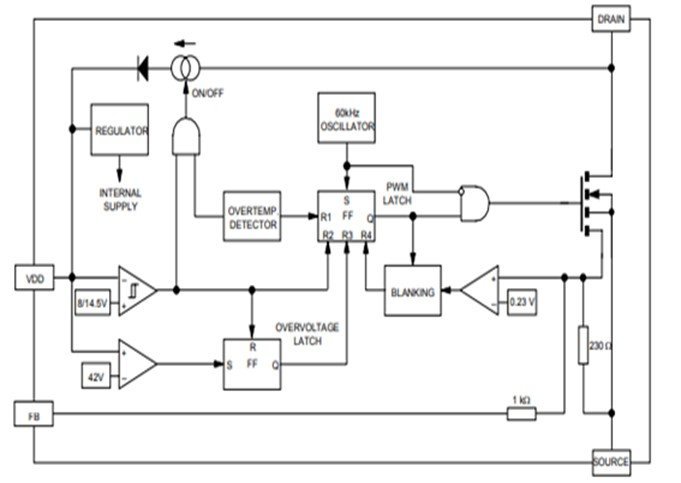
VIPER22A Block Diagram
The block diagram for the integrated circuit for better understanding of the components is provided for the visual down below.
VIPER22A SMPS Example Circuit
SMPS Power Supply
This section is an example guide of SMPS Power supply circuit using VIPER22A SMPS Controller IC. The circuit takes in 220-240 volts input power to give out 12V,1A of output at full load. The prototype is built in Power Supply design software provided by its own manufacturers. The schematic of the SMPS prototype is displayed for the show.
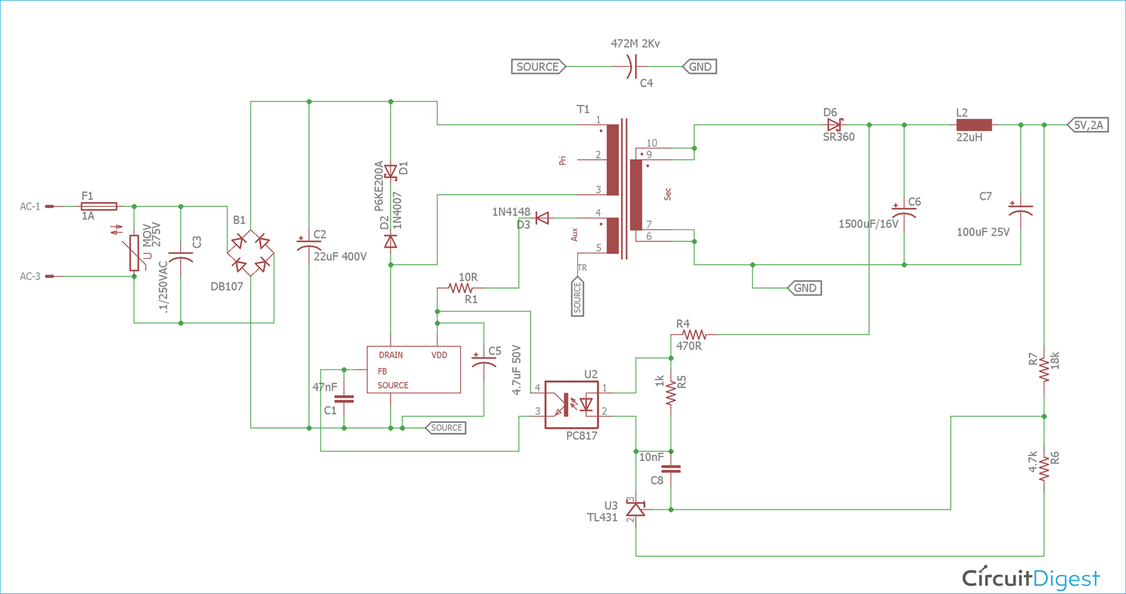
VIPER22A Circuit Components
The VIPER22A SMPS Power supply consists of different parts and sections. These are as follows and will be discussed in detail in the next section:
- Input surge and fault protection circuit
- Input Filter
- Full wave Rectifier
- Switching driver
- Clamper
- Magnetic and galvanic isolation.
- EMI filter
- Secondary Rectifier
- Filter Section
- Feedback mechanism.
Input surge and fault protection circuit
The fault protection circuit consists of a fuse and a Metal Oxide Varistor(MOV). As you can see through the schematic, F1 in series is a 1A, 250VAC slow blow fuse and MOV is a 275V, 7mm MOV. Whenever the input voltage shoots up more than the limit often called as voltage surge causes extreme current flow. In this situation, MOV becomes short to the fuse and the maximum inrush current flows through the slow blow fuse.
Input Filter
Following fault protection is the input line filter capacitor. A 250 VAC X-type line capacitor is connected to avoid unwanted line voltage noise generated in the circuit.
Full wave rectifier
The Analog input voltage is digitized through a 1A, 1000V DB107 full wave rectifier. The resultant digital signal is then filtered and DC level is smoothened using a 400V capacitor with 22uF capacitance.
Switching Driver
Next is the VIPER22A IC. The integrated circuit is connected to the transformer winding to get the input bias. The IC is embedded with high-power MOSFET that performs switching across the transformer. A diode i.e D3 changes the analog output to the DC output followed by the 10 ohms resistor to resist the inrush current. The output is then passed through the capacitor to smoothen the DC output ripple.
Clamper
The clamping circuit is responsible for clamping the voltage spikes which occur due the switching of transformer. Diodes D1 TVS diode works as a clamper & D2 ultra-fast recovery diode works as a blocking diode. The transformer serves as an inductor for the SMPS driver and produces voltage spikes in switching off cycle due to leakage inductance. This damages the driver. So to prevent that we have opted for P6KE200A and UF4007 and it clamps the output to 200V.
Isolation & EMI Filter
It is important to isolate the circuit magnetically to avoid stray currents. So we are using a ferromagnetic transformer with three windings i.e. Primary, Secondary and Auxiliary C1 is a Y-class 2kV capacitor. It is kept filtering and reduce the EMI interference caused by induction in the circuit.
Secondary rectifier & filtering
The component D6 in the schematic is the SB360 Schottky diode with 3A 60V ratings. We are designing a power supply with 2A output current. So the specified diode is being used. In the end, ripple removal from the DC voltage is done again using C6 and post LC filter (L2 & 7).
Feedback Mechanism
The feedback circuit is electrically isolated from the VIPER22A driver circuit due to the optocoupler PC817 (U2) because of optical communication instead of electrically. TL431 shunt regulator and R6, R7 that works like a resistor divider detects the output voltage. The shunt regulator has a reference potential of 2.5 volts. Our target output is 5 volts so whenever the output voltage gets to 5 volts the regulator attains 2.5 volts across its pin and controls the optocoupler which controls the VIPER22A driver circuit or TNY268PN. Otherwise, the switching is halted.
TNY268PN turns on the switching cycle and checks the enabling pin. In normal conditions it will keep working and counters the overvoltage problems. In faulty conditions the TNY268PN and feedback loop tries again till the conditions are normal. This trying loop is known as hiccup operating mode and this feedback mechanism in which the output voltage is carried back to the driver to continue the operations is known as flyback topology.
Alternate Options
- VIPER12A
- AP8012
VIPER22A Applications
- SMPS Circuits
- Low power systems
- Industrial Applications
- Battery Chargers
- Automobiles
VIPER22A 2D Diagram

Related Articles:
- output inductor design and calculation for SMPS
- MB102 Breadboard Power Supply module
- Boost Converter Proteus Simulation
- Buck Converter Proteus Simulation
- In-Depth 555 timer IC complete guide
- SG3525 Pulse width modulation controller IC
- Single Phase Voltage Source inverter simulation in Simulink
- Smart under and over voltage protection system for home
- Know all about Switch Mode Power Supply
- 18 volt transformer less power supply
- Transformer less power supply for microcontrollers
- UPS uninterruptible power supply circuit diagram
- Buck converter simulation using PSpice
wonderful and easy explanation, also post a good video for transformer design and sources to get it from, as per design
what is the output of the transformer voltage and current?
12v/1a, 5v/2a …
Is their any tool for transformer design
Your transformer polarity is incorrect for flyback circuits. Request you to make the correction, else newcomers may learn something wrong. You have currently made the main secondary winding in a forward-convertor configuration. For flyback, the polarity of the transformer (the dot) should be reversed. The tiny auxiliary winding (for powering the viper22a) may be left in the forward converter topology.
I received viper 22 A ic smps for service. Found viper 22 A busted & 47 mfd short at pin number 4. replaced two components but there is no output. any one can comment.