In this article, we will discuss electronics lab components and their working. First, we will provide a brief introduction to electronic lab components or equipment. After this, we will discuss the basic purposes of these components and their use in electronics lab experiments. In the electronic circuit lab, the primary piece of equipment that we usually deal with is the trainer board. A trainer board is essentially a collection of most of the electronic lab components that we typically require when working with logic circuits.
Components of Trainer Boards
There are three types of trainer boards present in the lab. All three should have the following:
- Breadboard
- Power Supply for ICs
- Logic Switches
- LED output
- Seven Segmented Display
- Clock
1. Electronics Lab Components: Breadboard
This is the first important part of electronics lab components. The most common circuits we come across in our everyday lives are in the form of printed circuit boards (PCBs). But every circuit starts off as an implementation on a breadboard. A breadboard is a prototyping board having an insulation material with a perforated top in which we can easily insert wires and components. The perforations in the board connect in a special manner through internal wiring at the bottom of the board. The fact that we just insert or place wires and components, not solder them, means that we can easily remove, replace, or alter their interconnections.
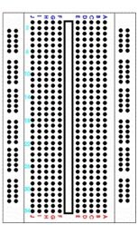
In contrast, to make changes to a PCB, a new PCB requires a design, which incurs costs in terms of both time and resources. Therefore, breadboards are ideal for testing and lab work since, in both cases, circuits undergo a lot of changes. Figure 1 shows the layout of a basic breadboard. In order to design and build large circuits, we can place two such trainer boards side by side, as we will see in some of the later labs.

Explanation
Figure 2a shows the manner in which the inner perforations connect. Each row of 5 holes is “shorted”. Each hole in a row connects to each other through an internal wire. The large rectangle in the center represents a grove. We need to note that the holes on one side of the grove do not connect to the holes on the other side.
Figure 2b shows the connections of the outer perforations. The holes are shorted column-wise, with no connections between the adjacent columns. Also, while the number of perforations in a column may vary with the length of the breadboard, there is always a break in connection at the half-way point in a column, as we can see in the figure. This means that each column is essentially split into two smaller columns.
2. Power Supply for ICs
In electronics lab components, the components that we will work with are mostly integrated circuits (ICs). There are several different types of ICs, each with its own unique functionality. Figure 3 shows the structure of a typical IC chip package. Every IC has a grove at the top, which determines its orientation.
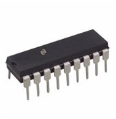
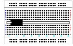
Figure 4 shows the manner in which we place an IC on the breadboard. The general rule is to ensure that the groove on the IC is pointing towards the left, as we can see in the figure.
Setting up an IC
ICs are active elements. This means that they need power before we can use it. Therefore, every IC, no matter what its functionality, will always have two special pins with labels for Vcc and Ground (or Gnd). Ground always connects to the GND supply of the trainer board, while Vcc connects to the 5V supply. Ignore the 12V and the -12V supplies on the board. We need to note that voltage is a relative quantity. The expression of voltage at any point can only be the difference between that point and the voltage at a reference point.
Thereference point that we will use is the ground. Ground is all the connections on the trainer board that we assume are at 0V. All the voltages on the trainer board are with reference to ground pins. For example, the pin with the mark +5V is at a voltage that is 5 volts greater than the ground pin. This also means that if the pin with a +5V mark is assumed to be at 0V, then the ground pin will be at -5V. When using multiple trainer boards, make sure that the ground pins of the trainer boards are short together to ensure that the reference voltage is the same throughout the circuit.
3. Logic Switches
Logic switches are the basic building blocks of electronics lab components. The inputs to a logic circuit consist of a collection of ON/OFF signals. The ON signal (or logic ‘1’) generates after applying +5V to an input pin. Whereas an OFF signal (or logic ‘0’) generation occurs by applying 0V to an input pin. Figure 5 shows the internal structure of a switch in the ON and OFF states. When the switch closes (by moving the switch down), it outputs +5V. When the switch opens (by moving it up), the output of the same pin is now 0V. This is “positive logic connection.” To provide these ON/OFF signals, the trainer boards have the following logic switches:
1. Inverting Switches (Set A/Set B)

These switches have two outputs. The first output is the normal output, which follows the convention as in the description above. The second (inverted) output is the inverse of the first output; that is, if the normal output is 5V, then the inverted output is 0V, and vice versa. The inverted output is typically denoted with an apostrophe (‘).
2. Non Inverting Switches
These switches have a single output, which follows the normal convention as stated above.
3. Debouncing Switches
When a normal switch is “thrown”, that is, when its state changes, the resulting output voltage does not immediately go to and stay at the new value. Rather, it oscillates between 5V and 0V for a short period before settling at a desirable output. In sensitive circuits, this will lead to the circuit producing incorrect results. A de-bouncing switch employs a circuit to remove these oscillations and produce a clean transition when we throw the switch.
4. LED Output
The outputs of logic circuits, like the inputs, consist of ON/OFF signals. We can verify them by using the LEDs available on the trainer boards. LED stands for Light Emitting Diode, a two-terminal device that only conducts in one direction, as is the case with a typical diode. They convert electrical energy into light energy. The conversion results in a drop in voltage across the terminals of the LED, which is typically around 2 V. LEDs offer a big advantage over traditional bulbs in that they consume a negligible amount of power. The disadvantage of LEDs is their inability to withstand high voltages or currents. Therefore, when using an LED, always connect a resistor (100-200 Ω) in series with it.
The LEDs present on the trainer board already have one terminal that connects to the ground, and the resistor connects to the other terminal internally. Therefore, we do not need to connect a resistor when using the LEDs on the trainer board. To test the output of an IC, connect it directly to the input terminal of an LED that is available on the trainer board. If an LED turns on, then the output state at that pin is ON (+5V). If it remains off, then the pin is in OFF state (0V). Remember to turn on the trainer board before using the LEDS (in case you are using an external supply to power up your circuit).
5. Seven Segment Display
The seven-segment display allows us to view the outputs in decimal form. It takes four inputs (binary) and, depending on their state, turns on LEDs in the display to show the corresponding digit. For example, if the input to the display is 0111, then the display will show the number 7. If the input to the display is a number >9 (1001 in binary), the display will not show a number. Instead, it will display a unique character corresponding to that binary input. To turn off the display, apply the input 1111 to it.
6. Clock
The trainer board provides a square wave that oscillates between a minima of 0V and a maxima of 5V. We call this a clock. The clock is useful to drive “sequential” logic devices, which we will come across in the later labs. Essentially, this clock serves the same purpose as the clock in our computers. The trainer board provides the option of varying the frequency of this clock, but the amplitude is fixed.
7. Power Supply
Sometimes, in electronics lab components, we may need to supply voltages other than those available on the trainer boards. For this purpose, we will be using a power supply (Figure 6). The power supplies present in the lab are able to provide two independent variable voltages ranging from 0V up to 30V. It also provides a fixed voltage supply of 5 V. Each voltage output block consists of a positive terminal (red) and a negative terminal (black). In some cases, a third terminal with the label GND (yellow or green) may be present, but we can ignore it. The voltage supplied by the power supply is essentially the voltage of the positive terminal with respect to the negative terminal. To generate positive voltages, the negative terminal shorts with the ground of the circuit, and voltage is obtainable from the positive terminal.
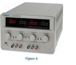
To generate negative voltages, the positive terminal shorts with the ground of the circuit, and voltage is obtainable from the negative terminal. The display will always indicate a positive value, but the actual sign of the output voltage depends on the manner in which we connect the terminals. Note that, in using multiple voltage outputs from a single supply or from multiple power supplies, all the terminals to be at 0V should be short together.
Using Power Supply
Voltage can be varied on the variable outputs of the supply by rotating the respective voltage knobs. Apart from the voltage knob, there is one for current as well. The purpose of this knob is not to generate current as current depends entirely on the voltage being supplied and the power being drawn by the circuit. This knob is used to limit current, that is, it controls the maximum amount of current that can flow from the output block. If current being drawn from the supply tries to increase beyond the limit, the red indicator LED turns on and the voltage being supplied drops even though the voltage knob is still in the same position. Since logic circuits draw a very small amount of current, it is a good idea to keep the limit to a small value.
8. Digital Multi Meter (DMM)
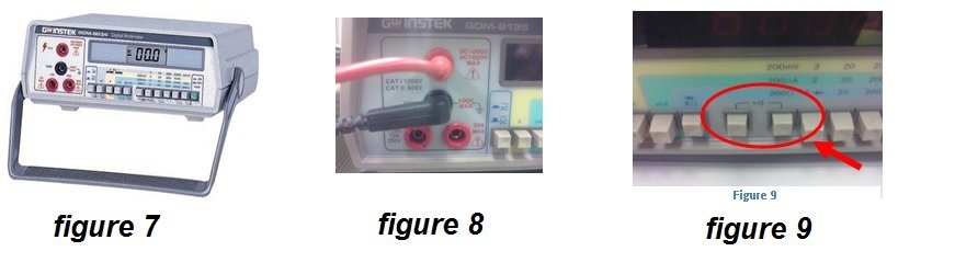
The multimeter (Figure 7), as suggested by its name, is used to measure multiple parameters in a circuit. It can be used to measure voltage, current, resistance, capacitance and it even has a mode for checking for short circuits. In logic circuits, you will typically be using only the voltage and the short circuit mode.
1. Voltage
The voltage mode is accessed by pressing the button marked
“V”. Similar to the principle of generation, voltages are measured as the voltage at the red probe with respect to the black probe. The probes are connected to the multimeter as shown in Figure 8. In most cases, the black probe is shorted with the ground of the circuit. However, for cases such as measuring the potential drop across a resistor, the probes may be placed at the terminals of the resistor while it is inside the breadboard. The value of potential drop being displayed may either be positive or negative and this can be used to determine the direction in which current is flowing in the resistor.
2. Short Circuit
The short circuit mode is accessed by pressing the three buttons marked in Figure 9. All three buttons should be in a pushed in state. In this mode, the two probes can be used to check if a short circuit exists between two points in a circuit. The mode works by checking if a closed loop is formed between the probes. A closed loop is a path in a circuit is one in which current can flow. This means that if two points are shorted together, current will flow between them. If there are not connected, then there is no closed path for the current to travel (open loop) and hence no current will flow.
9. Oscilloscope

The oscilloscope (Figure 10) is one of the most interesting pieces of equipment that we will be using in the lab. Although it can only measure voltages, it allows us to perform a large number of functions on the acquired data. It is particularly helpful in measuring voltages that change with time, as it is able to not only plot the wave form but also automatically measure many parameters that correspond with the wave. The probes of an oscilloscope are similar to the ones we can see in Figure 11. The small black clip connects to the ground of the circuit, whereas the larger gray part of the probe connects to the point whose voltage we need to measure.
In electronic lab, the typical DMM measures voltage whereas the use of an oscilloscope is to observe signal wave forms.
10. Function Generators
The use of a function generator (Figure 12) is to produce wave forms of variable frequency, amplitude, and offset. The generators in the lab are capable of producing sine waves, triangle/saw-tooth waves, and square waves. The principle of voltage generation is again similar to that of the power supply, in which the negative (black) clip connects to the ground and the voltage at the positive (red) clip oscillates with respect to it. While we may be familiar with the terms frequency and amplitude, offset is a relatively new yet equally important quantity. Without offset, a generated waveform oscillates about the 0V line, with the maximum and minimum voltages being A and -A (A = amplitude).

This means that for half the time period, the output voltage is positive, and for the remaining part, the output voltage is negative. If, for example, we add A volts, the maximum and minimum voltages become 2A and 0, respectively. Thus ensuring the output voltage is always positive. For an offset of -A, the output voltage is always negative. Any value of offset will thus result in a change in the maximum and minimum values of the output voltage.
Two observations should be made here. Firstly, an offset does not change the shape of the waveform since the voltage at each point in the wave is changed by the same relative amount. Secondly, in the case of a square wave, if the magnitude of the offset is < A, then the wave is still positive and negative for the same period of time as it would have been for a zero offset.
Conclusion
In conclusion, this article provides an in-depth overview of electronic lab components. It covers most basic components such as breadboard, ICs, logic switches, led output, clock, power supply, oscilloscope , seven segment display along with their uses in detail to help us better understand the concept. Hopefully, this article was helpful in expanding your knowledge.
You may also like to read:
- DC Motor Control with LabVIEW and Arduino – Tutorial 3
- PID Controller Design using Simulink MATLAB: Tutorial 3
- MPLAB XC8 Compiler – Write your First Program
- MB102 Breadboard Power Supply module – How to use it
- 4×1 Multiplexer Design in Labview: Tutorial 33
- Auto Power Supply Control System from 4 Different Sources Using PIC Microcontroller
This concludes today’s article. If you face any issues or difficulties, let us know in the comment section below.