PIC16F887 Microcontroller is an 8-bit microcontroller designed with RSIC CPU technology, which helps the microcontroller to give the maximum output using less power. It has a total of 40-pins and all these pins come in multiple packages to solve the requirement of small and modern circuits. 44 pin QFN and TQFP packages are also available. PIC16F887 provides all the modern protocol to the developers and due to its multiple pins, the most protocol can be followed at the same time without effecting others. The PIC has multiple usages with the industry and at commercial level due to its multiple A/D channels and internal clock.
PIC16F887 Microcontroller Pinout diagrams
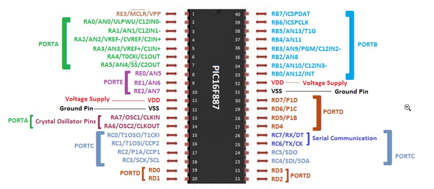
This microcontroller has three packages such as DIP, QFN, and TQFP. Pinout diagrams for these packages are shown here: This is a pin diagram for the 40 pin DIP package.
The diagram below shows the pin layout for QFN and TQFP packages.

Pin Configuration PIC16F887
PIC16F887 has a total of 40-pins and 44 pins packages with multiple features. We discuss the pin description and function of all these pins in this section.
GPIO Pins PIC16F877A Microcontroller
Digital Output
There is multiple output pin in the microcontroller. All pins come from five registers (A, B, C, D & E). They are compatible with any TTL/CMOS and ST devices. All GPIO pins give the maximum output voltage according to the applied power supply. All output pins are given below:
- PA0 – GPIO2
- PA1 – GPIO3
- PA2 – GPIO4
- PA3 – GPIO5
- PA4 – GPIO6
- PA5 – GPIO7
- PA6 – GPIO14
- PA7 – GPIO12
- PB0 – GPIO33
- PB1 – GPIO34
- PB2 – GPIO35
- PB3 – GPIO36
- PB4 – GPIO37
- PB5 – GPIO38
- PB6 – GPIO39
- PB7 – GPIO40
- PC0 – GPIO15
- PC1 – GPIO16
- PC2 – GPIO17
- PC3 – GPIO18
- PC4 – GPIO23
- PC5 – GPIO24
- PC6 – GPIO25
- PC7 – GPIO26
- PD0 – GPIO19
- PD1 – GPIO20
- PD2 – GPIO21
- PD3 – GPIO22
- PD4 – GPIO27
- PD5 – GPIO28
- PD6 – GPIO29
- PD7 – GPIO30
- PE0 – GPIO8
- PE1 – GPIO9
- PE2 – GPIO10
Digital Input: There are multiple input pins on the microcontroller and all of them come with an input pull-up resistor. In PIC16F887 the number of input pins is larger from all other pins and they can be used to wake up the microcontroller in case of sleep. These pins can operate at TTL/ST logic, which makes them compatible with all the other CMOS devices and peripherals. All input pins are listed below:
- PA0 – GPIO2
- PA1 – GPIO3
- PA2 – GPIO4
- PA3 – GPIO5
- PA4 – GPIO6
- PA5 – GPIO7
- PA6 – GPIO14
- PA7 – GPIO12
- PB0 – GPIO33
- PB1 – GPIO34
- PB2 – GPIO35
- PB3 – GPIO36
- PB4 – GPIO37
- PB5 – GPIO38
- PB6 – GPIO39
- PB7 – GPIO40
- PC0 – GPIO15
- PC1 – GPIO16
- PC2 – GPIO17
- PC3 – GPIO18
- PC4 – GPIO23
- PC5 – GPIO24
- PC6 – GPIO25
- PC7 – GPIO26
- PD0 – GPIO19
- PD1 – GPIO20
- PD2 – GPIO21
- PD3 – GPIO22
- PD4 – GPIO27
- PD5 – GPIO28
- PD6 – GPIO29
- PD7 – GPIO30
- PE0 – GPIO8
- PE1 – GPIO9
- PE2 – GPIO10
- PE3 – GPIO1
Interrupt Pins
Most of the modern applications/sensors required interrupt pin for fully operating. In PIC16F887 the total number of pins maybe 40 but it has only one external interrupt pin. This pin can be used to get the attention of the CPU of the microcontroller. Firstly, the microcontroller should be a program about this pin, because at default this pin won’t act as an interrupt pin.
- INT – GPIO33
PIC16F887 Serial Communication Ports
EUSART (Asynchronous): The use of this protocol has been increased nowadays in most modules and sensors. It has only two communication pins. One pin is used to send the data and the other one is for receiving the data. To use this protocol two devices only required some internal programming. Both these pins in PIC16F887 is given below:
- RX – GPIO26
- TX – GPIO25
EUSART (Synchronous): The synchronous method is mostly one way. It uses one clock and one data pin. The clock pulse and data are both controlled by the given instructions. Both pins are given below:
- CK – GPIO25
- DT – GPIO26
SPI: Most of the sensor uses the SPI protocol to communicate. In this communication, the multiple devices can be used with the same SPI pins. It uses four pins and all those pins are given below:
- SDI – GPIO23
- SDO – GPIO24
- SCK – GPIO18
- SS – GPIO7
I2C: This communication method uses only two pins but, in this method, at the same time only one device can send data. PIC16F887 has two pins for I2C protocol, from which one pin is used for clock pulse and the other is used for data transmission and receiving. Both these pins are given below:
- SDA – GPIO23
- SCL – GPIO18
ICSP: PIC16F887 has some ICSP pins within the GPIO which can be used to program the microcontroller in case of requirement. These pins are three in number and all of them are given below:
- ICSPCLK – GPIO39
- ICSPDAT – GPIO40
- VPP – GPIO1
- PGM – GPIO36
Analog to Digital Channels
There are 14 channels in PIC16F887 which can be used for analog to digital conversion. All those channels use only one 10-bit ADC. All ADC channels of PIC16F887 are given below:
- AN0 – GPIO2
- AN1 – GPIO3
- AN2 – GPIO4
- AN3 – GPIO5
- AN4 – GPIO7
- AN5 – GPIO8
- AN6 – GPIO9
- AN7 – GPIO10
- AN8 – GPIO35
- AN9 – GPIO36
- AN10 – GPIO34
- AN11 – GPIO37
- AN12 – GPIO33
- AN13 – GPIO38
Timer Modules Pins
In PIC16F887 there are three timers (Timer0, Timer1, Timer2), two of them are 8-bits and the last one is a 16-bit timer. All these timers can use both external and internal oscillator but timer1 can use a third oscillator at some GPIO pins. The timer1 and timer0 can calculate the external pulses through the external pins and timer one also has a control pin as a gate. All pins are given below:
- T0CKI – GPIO6
- T1OSO/T1CKI – GPIO15
- T1OSI – GPIO16
- T1G’ – GPIO38
Microcontroller Comparator Pins
There is a comparator with the PIC16F887 and it can be used as input and output of analog input signal. Their comparators use both inverted and non-inverted inputs of two signals and then convert them to their compared values. The compared signal can be used within the microcontroller. All these pins in PIC16F887 are given below:
- C12IN0(-) – GPIO2
- C12IN1(-) – GPIO3
- CVREF/C2IN (+) – GPIO4
- C1IN (+) – GPIO5
- C1OUT – GPIO6
- C2OUT – GPIO7
- C12IN2(-) – GPIO36
- C12IN3(-) – GPIO34
PWM Channels
Most of the devices required PWM to operate. The PWM pulse helps the device to variate their speed and voltages according to the given pulse. All PWM pin is given below:
- P1A – GPIO17
- P1B – GPIO28
- P1C – GPIO29
- P1D – GPIO30
Capture/Compare/PWM Pins
In PIC16F887 there is a CCP module which uses to compare the input signal then it compares to the given instructed signal. This module keeps comparing until the signal matches and then generates the output signal. This module mostly acts to use as PWM but it also uses to generate an event base signal.
- CCP1 – GPIO16
- CCP2 – GPIO17
PIC16F887 Power Pins
ULPWU: This pin can be triggered on the lowest voltages, that is the reason it is known as Ultra-Low-Power pin. This pin is used to wakeup the device with the lowest voltages.
- ULPWU – GPIO2
VREF: Every ADC uses the power supply voltages to convert the data but in some cases, the device starts getting unexpected data due to the analog transmitting device voltage. To solve this issue there are analog voltage input pins. On pin uses a non-inverted input and the other uses an inverted input as a reference voltage by analog output generating device. Both these pins are given below:
- VREF- – GPIO4
- VREF+ – GPIO5
Reset: There is a reset pin within the PIC16F887 which can be used by external devices or buttons to reset the device in case of requirement.
Power: PIC16F887 comes with multiple power pins. It has four power pins and all pins can be used at the same time. Power pins are connected internally. Two pins are for ground and the other two are for power input. Ground are common within the microcontroller and power pins are common too with each other. All power and ground pins are given below:
- VDD – Pin11, Pin32
- VSS – Pin12, Pin31
Oscillator/Clock: Oscillator is the basic requirement of every microcontroller. Every microcontroller requires clock input by which it will operate. In PIC16F887 there is an internal clock of 8MHz, whose frequency can be variate through programming. The frequency can be change from 31KHz to 8MHz. There are some external pins for oscillators which can also be used for an external oscillator. The external oscillator can be up to 20MHz only. The external oscillator pins can be used to receive the pulse of the internal clock too. All oscillator pins are given below:
- OSC1/CLKIN – GPIO13
- OSC2/CLKOUT – GPIO14
PIC16F887 Microcontroller Main Features
| FEATURES & SPECIFICATIONS | |
|---|---|
| CPU Architecture | 8-bit PIC |
| Internal Oscillator | 8MHz |
| External Oscillator | 20MHz |
| Operating Voltage Range | (2V – 5.5V) |
| GPIO PORTS | 36 I/O Pins |
| Interrupts | 1 |
| Timers | 3 – (Two 8-bit and one 16-bit timer) |
| Comparators | 2 |
| PWM | 2 CCP and 2-PWM |
| ICP | One ICP Pin |
| USART | 1-Channel |
| I2C | 1-Channel |
| SPI/MSSP | 1-Channel |
| ICSP/MSSP | Available |
| ULPWU | Available |
| Watchdog timer | Available |
| Self-Programming | Available |
| LAN | Not Available |
| CAN | Not Available |
| ADC | 14-Channel |
| SRAM | 368 b |
| FLASH (Program Memory) | 14Kb |
| EEPROM | 256 bytes |
PIC16F887 Microcontroller Programming
To start learning pic microcontroller programming, you should have a grasp on GPIO pins. Therefore, we have elaborated on all pins and their functions in previous sections. We can use either assembly language or c programming to program microcontrollers. We suggest you have a look on these getting started tutorials:
- pic microcontroller assembly language programming
- Pic microcontroller programming in c using Mikroc Pro for PIC
Tools for Programming
To start with programming you need the following software and hardware components:
- A compiler or IDE to write a program in assembly or C language: The main thing where you will type your first microcontroller program is a compiler or integrated development environment. The three most popular compilers used for pic microcontroller programming are MPLABX IDE, Mikro C for PIC and PIC CCS compiler. A compiler is used to generate a hex file that the user uploads to a microcontroller.
- Programmer or Burner: When you finish writing your code, you have a hex file that you want to upload to a microcontroller. We use a programmer or burner to upload binary files to pic16f866. Pickit3 is one of the best choices for code burning.
- Pic Development Boards: Development boards are optional but they make your development process very easy. Because they offer man on-board peripherals like GPIO connectors, Sensors, ADCs, etc.
We will update this section with programming examples in embedded C language in this section.
Alternative Options
PIC16F877A, PIC16F886, PIC16F84A, PIC18F2550, PIC18F46K22
PIC16F887 Microcontroller Block Diagram

Applications
- PIC16F887 uses in most of the industrial applications as a controlling device.
- This device has most of the sperate communication pin, which makes it the one the most efficient microcontroller in its family.
- It is an ideal microcontroller due to multiple A/D channels in automobile systems.
Other Microcontrollers:
ATMEGA32, ATMEGA16, ATTINY45, ATMEGA328P, PIC18F2550, PIC18F4550, ATTINY88, ATTINY85, PIC12C508, PIC18F46K22, PIC16F877A, Dspic30f2010
Ich bin Anfänger , habe mir ein Entwicklungsboard für Pic 16f887a bestellt. und suche jetzt alle Informationen für Programmierung.