In this guide on SPI communication, you will grasp the concepts of SPI communication protocol which is also known as Serial Peripheral Interface, is a digital communication protocol that is used to transfer data serially (one bit at a time) between two or more digital devices like microcontrollers, microprocessors, or other devices. Many analog devices like analog to digital converts, analog sensors, temperature sensors, and data converters also provide interfacing mode based on SPI communication. You can go through these two articles to get more practical exposure to this communication interface:
The most commonly used devices which communicate with microcontrollers over SPI bust are:
- SD Cards
- RFID Modules
- 2.4GHz wireless transmitter and receiver modules
SPI Communication Introduction
- It is a serial and synchronous interface. The synchronous interface means it requires a clock signal to transfer and receive data and the clock signal is synchronized between both master and slave.
- Unlike UART communication which is asynchronous.
- The clock signal controls when data is to be sent to the slave and when it should be ready to read.
- The only master device can control the clock and provide a clock signal to all slave devices.
- Data can not be transferred without a clock signal.
- Both master and slave can exchange data with each other.
- No address decoding is done.
SPI Connection Between Two Devices
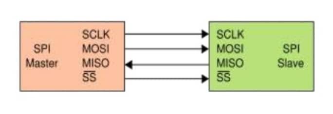
It is Full duplex synchronous communication. Both Master and Slave can exchange data with each other on the rising and falling edge of the clock signal. The Block diagram below shows interfacing with one Master and one Slave. SPI interface consists of either three or four signals. But in this article, We will see a general 4 wire interface.
The functionality of each signal is given here.
- SCLK or SCK pin : This signal provides a clock to Slaves and only Master can control clock signal. Note that this pin remains in idle state .i.e. inactive or tri-state when no operation is carried out.
- SS or CS : This is known as a chip select or Slave select pin. This line selects the slave to which Master want to transfer data.
- MOSI : It is a unidirectional pin. This stands for Master output and Slave input pin. As its name suggests, this line used to send data from master to slave.
- MISO: This is known as Master input and a Slave output. This line is used to send data from the slave to the Master.
In short, in this communication protocol, devices exchange data in master/slave mode. The master device is mainly responsible for the initiation of the data frame. The master device also selects the slave device to which data need to be transferred. Chip select line is usually used to identify or select a particular slave device.
Whenever a master device read to transmit data to slave or want to receive data from the slave, the master does so by activating the clock signal. Every master device sends data on the MOSI line and receives data through another line that is MISO. 
SPI Working Operation
As we mentioned earlier, the SPI bus consists of a single master and multiple slave devices. But SPI bus can be used in different configurations like a single master and a single slave as shown in the diagram below.
For some SPI devices, if only a single slave is used, a chip select pin can be connected with active low signal, but this feature varies for different SPI based devices.
SPI Protocol Data Transmission
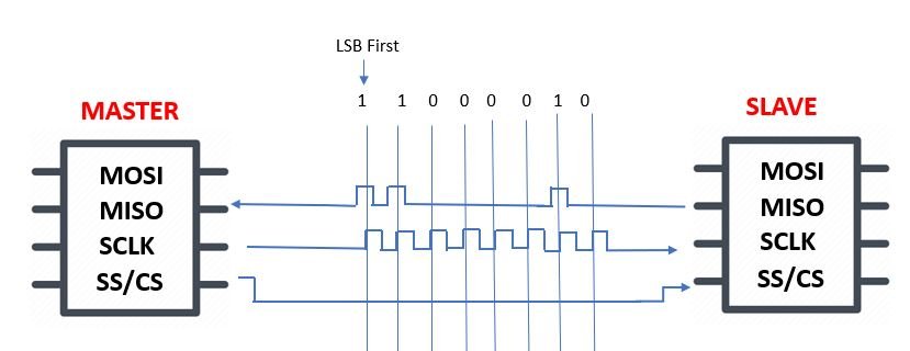
Now let us discuss the transmission of data through SPI protocol in a step by step manner.
- Firstly, the master outputs the clock signal as you can view in the figure below:

- Now to activate the slave, the master switches the SS/CS pin to a low voltage state.

- The data is sent to the slave along the MOSI line one bit at a time by the master. The slave reads the bits as they are received.
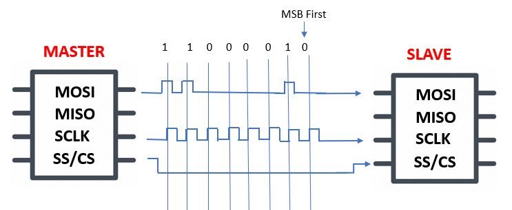
- If the master requires a response, the slave sends data to the master one bit at a time via the MISO line. The master reads the bits as they are received.
Different Configuration Modes of SPI Bus
- Typical SPI bus
- Daisy chained SPI bus
In typical SPI bus mode, only one master device can control multiple independent slave devices. However, an independent chip select signal is required for each slave device which is provided by the master device as shown here. The obvious pitfall of this configuration is that the number of chip select pins required with the master devices should be equal to the number of slave devices we want to use. This is also known as an independent slave configuration.

The Daisy chained SPI bus configuration is an improved version of the above-given model. It improves the previous configuration mode by reducing the drawback of typical SPI bus mode. In this mode, slave devices act like cooperative devices instead of independent devices. But the constraint of GPIO pins makes it difficult to implement a typical SPI bus method for embedded systems applications like with microcontrollers. Therefore, another method is daisy-chained mode which propagates data through devices connected in the chain or in series as shown in the figure.
In this configuration, only one chip select signal from the master device controls all slave devices and also all slave devices work on the same clock signal. But only the first slave device gets data from the master device directly, all other slave devices receive data on their input pin from the subsequent slave device as shown in the figure above. . Some devices come with Daisy chained and some with typical SPI mode configuration.
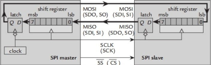
SPI Module Internal Structure
The data transmission between a master and a slave device generally consists of two shift registers as shown in the diagram here. These shift registers are usually of 8 bits size for both the master and the slave device.
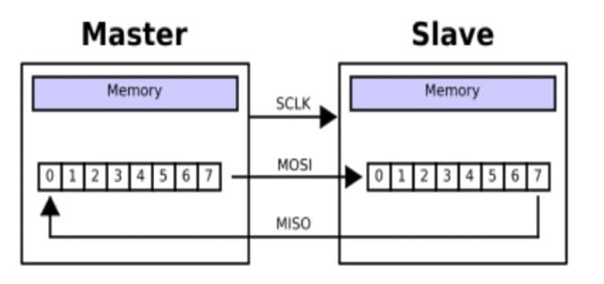
- It usually forms a circular buffer consists of two shift registers.
- In order to transfer data, a master device initiates the active high clock signal to a slave device and the frequency of the clock signal is less than or equal to the operating frequency of a slave device.
- The frequency range is between 1-70MHz for maximum SPI devices.
- After that, the master device makes the chip select signal active high to select a particular slave device to which it wants to transfer data commands.
- Each SPI clock transfers data in full-duplex mode.
- After selecting a slave, the master sends a start bit to the slave device over a MOSI line and slave reads this bit with the same line.
- The master device share date with the slave device using the shift register. After reading data, the slave device store the data from the shift register into memory and similar operation happen when the master wants to receive data from the slave.
Clock polarity and Phase
As I mentioned earlier, the master device is responsible for setting the clock frequency. But other than clock frequency, the master device also configures two things such as clock polarity and phase according to the data transmission.
Two registers/names are most commonly used and adopted by maximum vendors namely CPOL and CPHA. These names are just the conventions just by the most SPI devices vendors. The timing diagram of SPI communication along with clock phase and polarity signals are shown below.
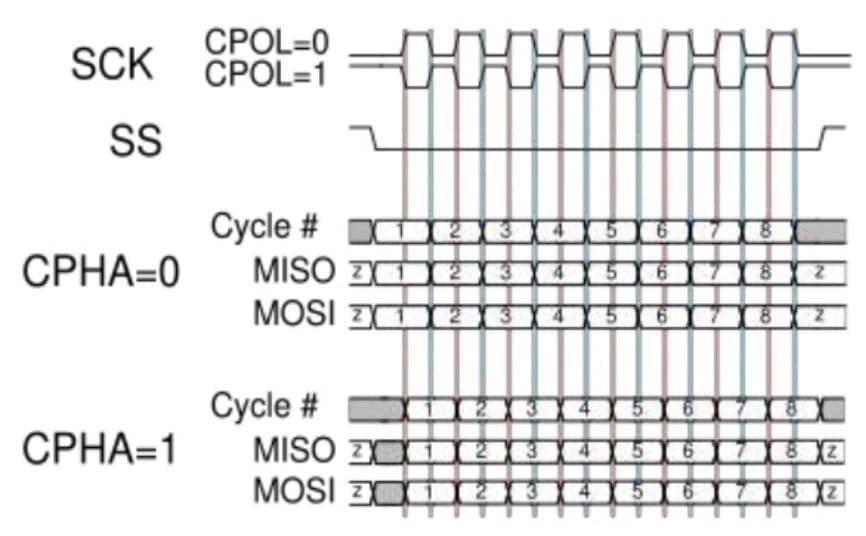
- During the active and idle state of the clock, the CPOL bit defines the clock polarity.
- On the other hand, the CPHA bit defines the phase clock. In other words, CPHA bit value sets either data will shift/sample on a positive edge of the clock or negative edge of the clock signal.
- The master device sets these two bits according to a slave device.
According to the values of these two bits, SPI communication can be in four modes given in this table.

Advantages
- It supports a full-duplex mode of serial communication.
- It provides higher throughput than I2C.
- The speed is faster than traditional asynchronous serial communication.
- Interfacing hardware is very simple. It just consists of a simple shift register.
- Power consumption is less as compared to I2C due to very simple hardware circuitry.
- Slaves do not require precision oscillator Because they use a clock from the Master device.
- No requirement of the transceiver circuit.
Disadvantages
- It requires more wires than I2C Communication. However, a three-wire variant of SPI exists but still, it consists of more wires than I2C.
- No hardware exists for flow control of data.
- No acknowledgment between Master and Slave. Even the master sends data to no device without noticing it.
- Only one master device is available at a time.
- It supports only short distance communication as compared to RS485, CAN and LIN communication.
- This communication requires slave select (SS) or chip select line for each slave device. It can create an issue if we are using a large number of slave devices.
SPI Communication Applications
- It is available to interface bare-metal embedded devices like microcontrollers with many peripheral devices like ADC modules, DAC, Temperature sensors and pressure sensors.
- External memory devices like a flash, Memory cards, and EEPROM also interface with microcontroller based on SPI.
- Many liquid crystal displays, OLEDs, TFT displays also used this communication protocol to interface with embedded devices.
Why SPI communication is used?
- Usually, Embedded system engineers use this communication protocol when they want to transfer fast data between two digital devices and a small number of input-output pins are available.
- In embedded systems due to constraints of less number of GPIO pins, we use serial peripheral interface to transfer data between two devices by using the minimum number of GPIO pins.
- SPI communication saves us wiring pins and also reduces the cost of hardware.
- This protocol can be implemented very easily and quickly with fewer I/O pins.
- It has a serial interface and a single master can control multiple slave devices to transfer data between each other.
- The only disadvantage of this is slower communication or data transfer rate. However, it is used in those applications where real-time data transfer is not mandatory.
Other Serial Communication Tutorials:
Microcontroller based Communication Tutorials:
- SPI Communication TM4C123
- I2C Communication TM4C123G Tiva C Launchpad
- ESP32 SPI Tutorial Master Slave Communication Example
- UART Communication TM4C123 Tiva C Launchpad
- SPI Communication with PIC microcontroller
- I2C Communication using PIC Microcontroller
- UART Communication with Pic Microcontroller
- UART Serial communication with MSP430 microcontroller