PIC18F2550 microcontroller is an 8-bit microcontroller designed by MICROCHIP. It is one of the cheapest microcontrollers of PIC18FXXXX series. It is popular due to its performance, cheapness and multiple features. PIC18F2250 microcontroller can interface directly with the other PC. It has multiple helping material on the internet due to its popularity and that is one the reason most of the developers and engineers use it. The microcontroller can keep the peripheral still active when the CPU core is on stand by and usage of internal oscillator also lead the controller to save up to 90% power saving.
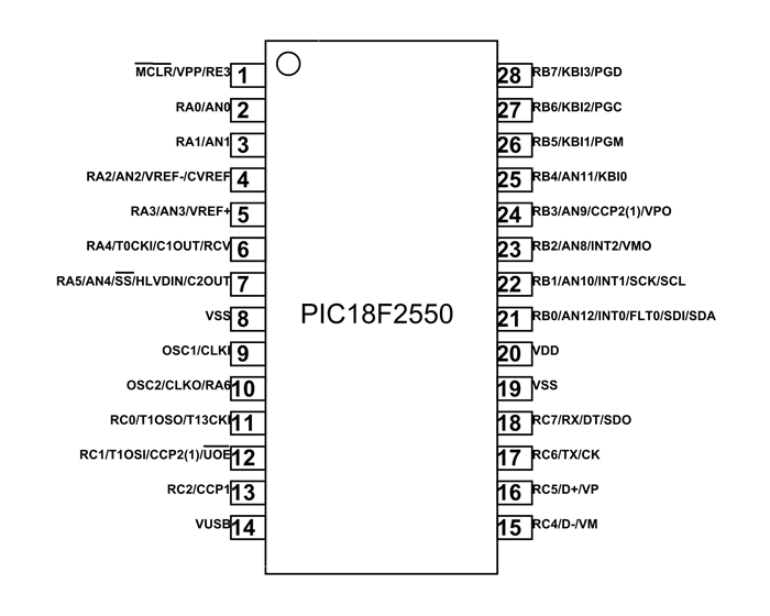
PIC18F2550 Pin Configuration
The pinout diagram including details of all pins and peripherals is listed below:
PIC18F2550 Features and Peripherals
In this section, we will see all the features and details of built-in features available.
DIGITAL OUTPUT PINS
The microcontroller has four GPIO ports (A, B, C and E). Instead of E, all ports provide the output function. The output pin attaches to the port A and B gives the TTL logic but the port C output comes in ST logic. The output pins on PIC18F2250 are:
- RA0 – GPIO2
- RA1 – GPIO3
- RA2 – GPIO4
- RA3 – GPIO5
- RA4 – GPIO6
- RA5 – GPIO7
- RA6 – GPIO10
- RB0 – GPIO21
- RB1 – GPIO22
- RB2 – GPIO23
- RB3 – GPIO24
- RB4 – GPIO25
- RB5 – GPIO26
- RB6 – GPIO27
- RB7 – GPIO28
- RC0 – GPIO11
- RC1 – GPIO12
- RC2 – GPIO13
- RC6 – GPIO17
- RC7 – GPIO18
Check this tutorial : How to use GPIO Pins of Pic microcontrollers
DIGITAL INPUT PINS
In PIC18F2550 the number of input pins is more than any other pins. Every port comes with input capability. Input pins on port A & B all input pins can be operated with TTL input but in port C (RC4 and RC5) can only operate with TTL input other pins on port C and E required ST logic to operate otherwise it could cause a problem for the microcontroller program to understand and operate properly. List of all input pins are:
- RA0 – GPIO2
- RA1 – GPIO3
- RA2 – GPIO4
- RA3 – GPIO5
- RA4 – GPIO6
- RA5 – GPIO7
- RA6 – GPIO10
- RB0 – GPIO21
- RB1 – GPIO22
- RB2 – GPIO23
- RB3 – GPIO24
- RB4 – GPIO25
- RB5 – GPIO26
- RB6 – GPIO27
- RB7 – GPIO28
- RC0 – GPIO11
- RC1 – GPIO12
- RC2 – GPIO13
- RC4 – GPIO14
- RC5 – GPIO15
- RC6 – GPIO16
- RC7 – GPIO17
Read this guide: USE INPUT OUTPUT PORTS OF PIC18F452 MICROCONTROLLER
INTERRUPT Feature PIC18F2550
Every external device requires to interrupt function in case of getting the attention of CPU and PIC18F2550 has three interrupt pins which can be used to receive the input signal to generate the interrupt within the microcontroller. Interrupt pins are:
- INT0 – GPIO21
- IN1 – GPIO22
- IN2 – GPIO23
Read this interrupts related article: How to use external interrupt of PIC18F452 microcontroller
EUSART ASYNCHRONOUS PINS
Nowadays most of the systems required serial communication systems and the Eusart Asynchronous serial communication system is one of the most popular systems for serial communication. It has separate data transmitting and receiving pins and both can be used at the same time.
- RX – GPIO18
- TX – GPIO17
SPI Communication PIC18F2550
The controller some times requires external modules to perform communication, and some of them use the SPI communication method. It is known as a three-wire communication system which uses two data wires, one clock pulse wire and a third wire know as slave select, which is used in the case of multiple peripherals. SPI pins on PIC18F2550 are:
- SDO (data-out) – GPIO18
- SDI (data-in) – GPIO21
- SCK (clock-pulse) – GPIO22
- SS’ (slave-select) – GPIO7
I2C Communication PIC18F2550 Microcontroller
It is a two-wire serial communication but it is one-way. It uses two wires one is used for clock pulse and others will be used for data transmitting and receiving data. The clock pulse helps the controller to use the multiple peripherals at the same time. I2C pins in PIC18F2550 are given below:
- SDA – GPIO22
- SCL – GPIO23
EUSART SYNCHRONOUS PINS
The IC has multiple ways to program but it can be programmed through synchronous serial programming. To program the controller serially three pins will be used, the first one for the clock, second for data transmit/receive and third one for programming power input.
- VPP – GPIO1
- CK – GPIO17
- DT – GPIO18
ICSP Serial Programming Pic18f2550
It is known as in-circuit serial programming, which uses a special programming circuit designed by the company to MICROCHIP to program the microcontroller using the HEX file of the program. In this process, 6-pins will be used. All these pins are listed below:
- MCLR’ – GPIO1
- VDD – GPIO20
- VSS – GPIO19
- PGM – GPIO26
- PGC – GPIO27
- PGD – GPIO28
USB Communication Pins
In PIC18F2550 USB can be connected directly to the microcontroller. Pic contains full speed and half speed USB interface. The USB can be connected through using the internal transceiver or external transceiver. The internal transceiver can be connected to the external USB interface but it also has the capability of using the external transceiver in case of requirement. The pins for both transceivers are given below:
EXTERNAL TRANSCEIVER:
- RCV – GPIO6
- VMO – GPIO23
- VPO – GPIO24
- UOE’ – GPIO12
- VM – GPIO15
- VP – GPIO16
INTERNAL TRANSCEIVER:
- VUSB – GPIO14
- D- – GPIO15
- D+ – GPIO16
PIC18F2550 TIMERS
There are a total of four-timer in PIC18F2550. One timer (Timer0) is of 8-bits and other three (Timer1, Timer2, Timer3) are of 16-bits. In PIC18F2550 the Timer1 can use the external oscillator, separate from the oscillator of the microcontroller. Timer 1 and timer 3 are the only timers which can be operated with external input signal the Time0 and Timer2 only operate internally:
- T0CKI (Timer0 external clock input) – GPIO6
- T1OSO (Timer1 oscillator output) – GPIO11
- T13CKI (Timer3 external clock input) – GPIO11
- T1OSI (Timer1 oscillator input) – GPIO12
HLVDIN PIN
It is a safety providing pin to the controller. By this user will be able to initialize the range of voltage within the microcontroller from where the device will be trip off. The input on this pin will be an analog input signal which will be able to generate the interrupt.
- HLVDIN – GPIO7
ANALOG TO DIGITAL CHANNEL
Analog to Digital converter becomes the need of every digital circuit because multiple sensors and peripheral give the output in analog form and microcontroller required analog converter channel to operate on that data. In PIC18F2550 there are total 10 A/D converting channels of 10-bits. These all channels can convert 10 analog input signals to a digital signal and then it stores/use it according to the instructions given in the program. The ADC pins in PIC18F2550 are listed below:
- AN0 – GPIO2
- AN1 – GPIO3
- AN2 – GPIO4
- AN3 – GPIO5
- AN4 – GPIO7
- AN8 – GPIO23
- AN9 – GPIO24
- AN10 – GPIO22
- AN11 – GPIO25
- AN12 – GPIO21
VREF PINS
In PIC18F2550 the ADC is smart because of VREF pins. There are two Vref pin pins, one of them is used to describe the maximum voltage of input analog signal and the second one will be used for input of minimum voltage of analog input signal. By this way, the ADC only gives the output of values within the range given by VREF. The Voltage reference pins are:
- VREF+ – GPIO4
- VREF- – GPIO5
COMPARATOR Module
There are two comparators within the microcontroller. These two comparators can compare multiple inputs. Their inputs can be takes by using any analog input signal from AN0-AN4. The output voltage can be compared on the VDD or separate comparator voltage reference can be provided on the comparator reference pin.
- CVREF – GPIO4
- CV1OUT – GPIO6
- CV2OUT – GPIO7
CAPTURE/COMPARE/PWM Module PIC18F2550
In this microcontroller, there are two capture/compare/PWM pins. This internal module uses Timer1 and Timer3 and allows the device to generate the output at a specific time. This module allows the controller to generate PWM of the desired duty cycle by using timers and Prescaler. The output pins of this module in PIC182550 are:
- CCP1 (Output) – GPIO13
- CCP2/RC1 (Input/Output) – GPIO12
- CCP2/RB3 (Input/Output) – GPIO24
- FLT0 (Fault) – GPIO21
By default, RB3 will give the output but RC1 and RB3 can be differentiated from the program internally. Fault detection pin is used to initialize the minimum fault active period within CCP1 (comparator 1 output). Read these PWM related tutorials:
RESET PINS
PIC18F2550 has an external reset pin which can be used to totally reset the microcontroller. The pin is an active low pin and can be operated with a button or any ST logic state device.
- MCLR’ – GPIO1
POWER INPUT PINS
The PIC has three power pins; one is used for power input and the remain two are ground pins used to make the common ground and they are also common within the controller. The power and ground pin of PIC18F2550 are:
- VSS – GPIO19, GPIO8
- VDD – GPIO20
OSCILLATOR/CLOCK PINS
Every microcontroller required a clock pulse to operate. PIC18F2550 comes with an internal clock from 32KHz to 8MHz and it can be calibrated at a different level through instructions. To use the clock up to 48MHz the controller provides two clock input pins, one for input and second for output. Both pins are:
- OSC1/CLKI – GPIO9
- OSC2/CLKO – GPIO10
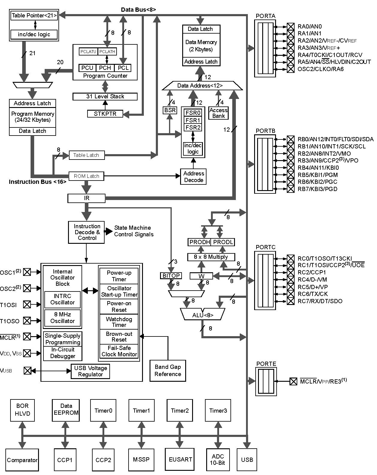
BLOCK DIAGRAM PIC18F2550 Microcontroller
Here’s the block diagram of PIC18F2550:
PIC18F2550 Microcontroller Programming
To start learning pic microcontroller programming, you should have a grasp on GPIO pins. Therefore, we have elaborated on all pins and their functions in previous sections. We can use either assembly language or c programming to program microcontrollers. We suggest you have a look on these getting started tutorials:
- pic microcontroller assembly language programming
- Pic microcontroller programming in c using Mikroc Pro for PIC
Tools for Programming
To start with programming you need the following software and hardware components:
- A compiler or IDE to write a program in assembly or C language: The main thing where you will type your first microcontroller program is a compiler or integrated development environment. The three most popular compilers used for pic microcontroller programming are MPLABX IDE, Mikro C for PIC and PIC CCS compiler. A compiler is used to generate a hex file that the user uploads to a microcontroller.
- Programmer or Burner: When you finish writing your code, you have a hex file that you want to upload to a microcontroller. We use a programmer or burner to upload binary files to pic16f866. Pickit3 is one of the best choices for code burning.
- Pic Development Boards: Development boards are optional but they make your development process very easy. Because they offer man on-board peripherals like GPIO connectors, Sensors, ADCs, etc.
We will update this section with programming examples in embedded C language in this section.
APPLICATIONS
- It is used with those devices which required interface with PC.
- Most of the smart application uses PIC18F2550 because it fills almost all the communication protocol of most of the applications.
Memory model PIC18F2550
PIC18F2550 has 32KB memory which is given below:
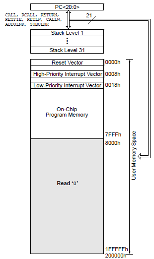
2D Diagram
