In this tutorial, I will explain the workings of a low-pass filter. The purpose of a low-pass filter is to allow only the lower frequencies to pass through the circuit and block the higher frequencies. At the start, we will provide a brief and concise introduction to filters, specifically low-pass filters, and bode plots with an explanation of the output they will show. After that, we will simulate the circuits using PSpice with the step-by-step approach to simulate a circuit, and then we will compare the results with the theoretical discussion (which should be the same). At the end of the tutorial, we have provided an exercise for you to do on your own, and in the next tutorials, we will assume that you have done those exercises, and we will not explain the concept regarding them.
Introduction to Low-Pass Filters
A low-pass filter is such a filter that only allows frequencies with lower magnitude to pass through it and blocks the higher frequencies, as the name suggests. The limit of the frequencies up to which the circuit allows is known as the critical frequency and is given by the formula.
This frequency is present at -3 dB of the maximum magnitude, which is 0.707, or 70% of the maximum magnitude. The output plot in frequency domain, or the bode plots of a simple low-pass filter, is given in the figure below.

How to Design and Simulate Low-Pass Filter in PSpice
Let’s design a simple circuit for a low-pass filter in this tutorial, with a few details that we provide as an exercise. Open the PSpice design manager on the PC by typing design manager in the search bar. From the design manager, click on the run schematic button to open a new blank schematic, as shown in the figure below.

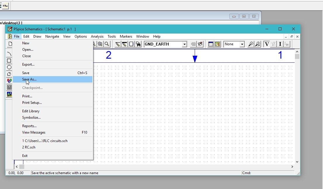
After opening the new schematic, before jumping into designing, first save the schematic by clicking on the file button at the top left corner and then selecting save as so that we can access it anytime in the future. Refer to the figure below.
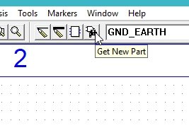
Click on the Get New Part icon at the top bar of the schematic window in order to search for the components that are needed for circuit design.
Placing Components
In the Get New Part window, type ‘Vac’. It will display an AC source available in PSPICE. From that list, select a simple AC source, as shown in the figure below.

Again, open the Get New Part window, and in the part name block, type C. Select the capacitor from the list given and then click on Place & Close, as shown in the figure below.

Again, open the Get New Part window, and in the part name block, type R. Select the resistor from the list given and then click on Place & Close, as shown in the figure below.

The next step is to place a ground. Do the same again, and in the part name type GND and select the ground, and then click on Place & Close as shown in the figure below.

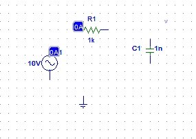
The components placed in the schematic window are shown in the figure below.
Click on the draw wire icon at the top bar of the schematic window in order to connect the already placed components for circuit design, as shown in the figure below.

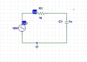
Complete Circuit Diagram
Connect all the components to complete the circuit diagram, as shown in the figure below.
On the top of the schematic window, click on the Voltage/Level Marker button, as shown in the figure below.

Place it at the output capacitor and at the input node, as shown in the figure below.
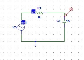
The next step is to set the attributes of the input AC supply. Double-click on the AC supply we connected in the circuit previously and set the magnitude of the voltage of the supply to 10 V and the DC voltage to 0 V, as shown in the figure below.

The only adjustable attribute in the AC supply is the magnitude of the AC voltage; leave all other attributes as is. The DC attribute is used to adjust the offset of the AC voltage. Its requirement is not in this experiment, hence it is left at 0.
Set the value of the capacitor according to the requirements of the circuit by double-clicking on the component. Now, change the value to 3u and then click Save Attr, but we are leaving the value in this experiment as is.
Simulation Setup
The next step is to adjust the properties of the simulations in order to produce a graph of the voltage at the marker. Click on analysis and then click on Setup, as shown in the figure below.

A window will appear. Click on the AC Sweep block on the window and adjust the properties of the window according to the requirements. Refer to the figure below.

Change the start and end frequencies in the property window according to the portion of the graph to be observed. If we have interest in checking the voltage on a specific wire in spite of checking it at a node, double-click on the wire, and in the window that appears as a result, we will type the name of the wire to label it with, as shown in the figure below.

Simulation
Now comes the simulation part. Click on the analysis at the top bar of the schematic window and then click on simulate, as shown in the figure below.

The output voltage at the capacitor node is displayed in the figure below.
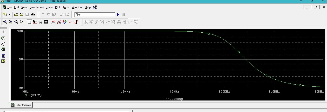
From the output, it is obvious that the circuit simulated is a low-pass filter. Above is the bode plot (frequency domain plot) of the circuit. At lower frequencies, the circuit is allowing the voltage to pass through it, and at higher frequencies, it drops to zero. Also, the results are in accordance with the theoretical introduction.
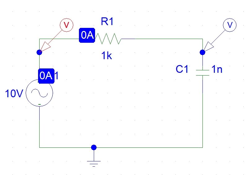
Connect another voltage marker at the input of the AC source to see the AC sweep of the source along with that of the capacitor, as shown in the figure below.
The output after connecting the voltage marker at the input is also shown in the figure below.

The green line at the top represents the input AC sweep of the AC source connection. The straight line represents that the input source is constant (neither increasing nor decreasing with time), unlike that of the capacitor voltage. In the frequency domain, we can say that the input source is allowing all the frequencies to pass straight through it.
Exercise
- Try doing the frequency domain analysis of any of the circuits we have done previously.
Conclusion
In conclusion, this tutorial provides an in-depth overview of how to design and simulate a low-pass filter in PSpice. It covers step-by-step procedures with clear and concise explanations and examples to help us better understand the concept. You can utilize this concept to design and simulate more complex filters in PSpice. Lastly, an exercise is provided to reinforce the concept of low-pass filter design in this tutorial. Hopefully, this article was helpful in expanding your knowledge in regards to designing and simulating in PSpice.
You may also like to read:
- ESP8266 NodeMCU Erase Flash Memory Perform Factory Reset
- Arduino Uno Introduction, Pinout, Examples, Programming
- Raspberry Pi Pico W Wi-Fi Manager Web Server using MicroPython
- BeagleBone Black Pinout, Pin Configuration and Features
- ESP32 WebSocket Server using Arduino IDE – Control GPIOs and Relays
- Raspberry Pi 4 Pinout, Features and Peripherals
- STM32 DMA Tutorial How to Use Direct Memory Access (DMA) in STM32
This concludes today’s article. If you face any issues or difficulties, let us know in the comment section below.