In this in-depth guide, we will see how to interface 74HC595 shift register with pic microcontroller. 74HC595 is a serial-in and parallel-out shift register. It takes data serially and provides data parallelly through 8 data lines. In this tutorial, we will see how to send data to 74HC595 from PIC16F877A to control eight LEDs. We will provide example codes with MPLAB XC8 compiler and MikroC Pro for PIC. Without using a shift register, we will typically need 8 output pins of PIC16F877A microcontroller to control 8 light-emitting diodes.
Recommended Components
The following components are used in this project or are helpful for building it with a PIC microcontroller.
| Component | How it’s used in this project | Buy on Amazon |
|---|---|---|
| PIC16F877A microcontroller | Host MCU that clocks serial data into the 74HC595. | Check Price |
| PICkit 5 programmer/debugger | Flashes the compiled firmware onto the PIC and debugs it. | Check Price |
| 74HC595 shift register | Serial-in parallel-out shift register expanded from three PIC pins. | Check Price |
| Breadboard | Solderless base for wiring the PIC to the shift register. | Check Price |
| Jumper Wires | Connect the data, clock and latch lines between parts. | Check Price |
As an Amazon Associate we earn from qualifying purchases. Prices and availability are accurate as of the date/time indicated and are subject to change.
Why do we need to use 74HC595 shift register?
But the question is why do we need a shift register IC? As you know that microcontrollers such as PIC16F877A comes with limited number of general-purpose input-output pins. We can use shift registers such as 74HC595 to save microcontrollers pins.
For example, in the last tutorial, we have seen how to interface a 7-segment display module with pic microcontroller. In that tutorial, we had to use 8 GPIO pins to control one 7-segment display and similarly, for 4-digit seven-segment we had used 12 GPIO pins. But if you use a 74HC595 shift register IC, we can reduce the number of pins to maximum four to control the 4-digit seven-segment device.
Let me give you another example of an LED matrix interfacing with pic microcontroller. For example, if we want to interface an 8×8 LED matrix with PIC16F877A microcontroller, we have used 16 GPIO pins of PIC16F877A. But if we use 74HC595 to control 8×8 LED matrix with help PIC16F877A microcontroller, we can achieve the same function with 5 GPIO pins.
That’s enough of reasons that should convince you about shift register use.
74HC595 shift register Introduction
Typically, two types of shift registers are used such as serial-in and parallel-out (SIPO) and parallel-in, serial-out (PISO). 74HC5959 is a SIPO types and one of the popular chips of PISO type is 74HC156.
PISO type of shift registers are used to collect data from many input pins such as push buttons. On the other hand, SIPO are used to drive multiple output devices with few output pins of microcontroller.
The operating voltage range is 2-6 volts. Therefore, we can provide same 5 volts power supply to PIC16F877A and this IC.
Pinout Diagram
It is a 14 pins IC. 9 pins are parallel output pins from Q0-Q7 and ~Q7. ~Q7 pin is used for cascading two or more shift registers. For instance, as you know 74HC595 is a 8-bit shift register, what if you need a 16 bit shift register. We can use this pin for cascading two ICs to make 16-bit serial-in, parallel-out shift register. This diagram shows the pinout.
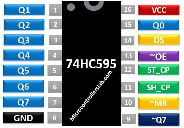
This table lists working of each pin and how to connect these pins with PIC16F877A microcontroller
| Pin Number | Pin Nmae | Function |
|---|---|---|
| 1-7, 9, 15 | Q0-Q7 and ~Q7 | 8-bit output register and ~Q7 used for cascading |
| 14 | DS | Serial Data input |
| 13 | ~OE | Enable pin ( Active low) |
| 10 | ~MR | Reset pin (Active low) |
| 11 | SH_CP | latch pin ( sends data to output pins from shift register) |
| 12 | ST_CP | Clock signal for serial data transfer to DS pin |
| 8 | Ground | Ground terminal |
| 16 | Vcc | Connect 5 volts for power supply |
How it works?
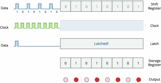
As mentioned earlier, the internally 74HC595 shift register consists of two registers such as shift register and storage register. Both are 8-bit wide. The first one is responsible to accept data input on every positive edge of the clock and it keeps receiving data. But data from the shift register transfer to the storage register only when we apply an active high signal to latch input pin.
Therefore, we will apply data, clock and latch signal from PIC16F877A microcontroller. First, we will send 8-bit data serially and a clock signal from microcontroller on DS and ST_CP ( clock) pins. After transferring 8-bit data to the internal shift register, we send latch signal from Pic microcontroller to transfer data to storage register(output register)
For further information on 74HC595 serial shift register, check this link:
Schematic Diagram
In this example, we will control 8 LEDs with a 74HC595 shift register and PIC16F877A microcontroller. To interface 74HC595 with PIC16F877A microcontroller, we will use three GPIO pins. All three pins will be used as a digital output pin. These three pins are clock, data and latch pins.
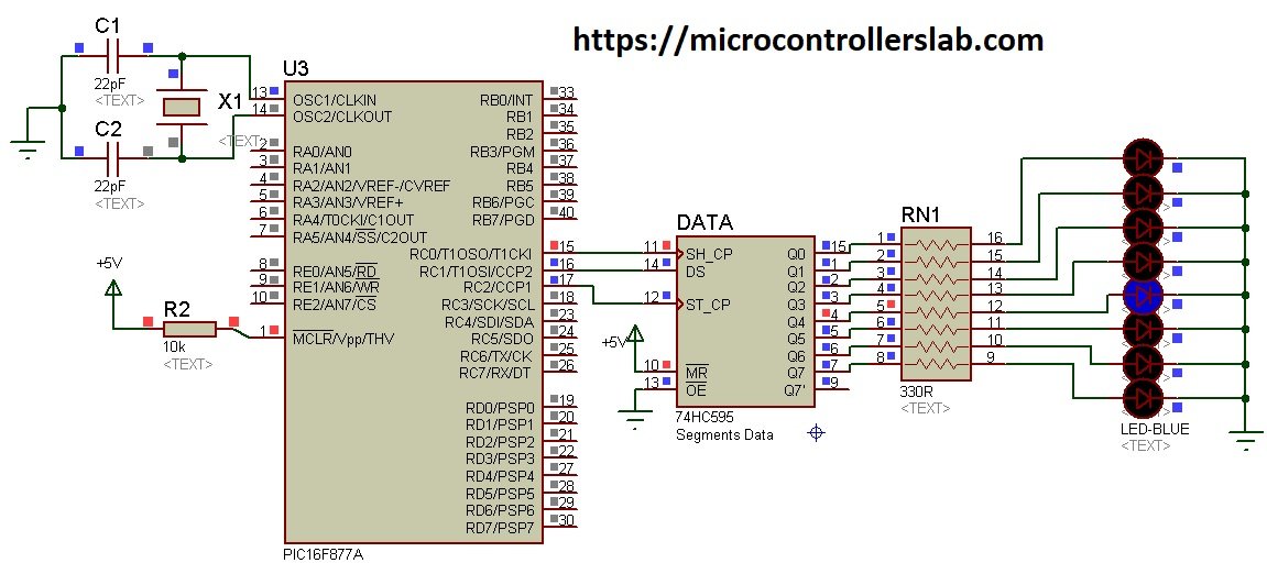
As we mentioned earlier, shift register takes one-bit data serially on every positive edge transition of clock signal and shift register holds this data. To send shift register data to output register or output pins (Q0-Q7), we should activate latch pin by providing positive edge pulse. Therefore, one pin of PIC16F877A microcontroller provides latch signal.
Connections PIC16F877A and 74HC595
Now make connections of PIC16F877A with 74HC595 shift register according to this table. We connect the enable pin (~OE) with ground which activates this IC. Because it is active-low pin. We can also control this pin via microcontroller pin. But just to save PIC16F877A pin, it is better to provide hardwired signal by directly connecting it with ground.
LEDs connections
Connect eight output pins with LEDs through current limiting resistors. This circuit will turn on all these LEDs sequentially with some delay.
Crystal Oscillator
We must use a 8MHz external crystal oscillator. Unlike other pic microcontroller, PIC16F877A don’t have internal oscillators. Therefore, connect external crystal along with two 22pF capacitors.
MikroC Code
This code is for controlling LEDs with 74HC595 serial shift register.
This code is written using MikroC for Pic compiler. Create a new project with MikroC compiler by selecting PIC16F877A microcontroller and set frequency to 8MHz. If you don’t know how create new project in mikroC, we suggest you read this post:
After creating new project, go project>>edit project and set configuration bits setting to CONFIG : $2007 : 0x2F4A.
sbit DATA_pin at  PORTC.B1;
sbit LATCH_pin at PORTC.B2;
sbit CLCOK_pin at PORTC.B0;

void clock_signal(void){
   CLCOK_pin = 1;
    delay_us(500);
   CLCOK_pin = 0;
    delay_us(500);
}
void latch_enable(void)
   {
    LATCH_pin = 1;
    delay_us(500);
    LATCH_pin = 0;
    }
void send_data(unsigned int data_out)
{
    int i;
    unsigned hold;
    for (i=0 ; i<8 ; i++)
    {
        DATA_pin = (data_out >> i) & (0x01);
        clock_signal();
    }
    latch_enable(); // Data finally submitted
}
void main()
{
  TRISC.B0 = 0; // Set  DATA_pin as output pin
  TRISC.B1 = 0; // Set  CLCOK_pin as output pin
  TRISC.B2 = 0; // Set LATCH_pin as output pin
  while(1)
      {
        send_data(0b00000000);
        delay_ms(200);
        send_data(0b10000000);
        delay_ms(200);
        send_data(0b01000000);
        delay_ms(200);
        send_data(0b00100000);
        delay_ms(200);
        send_data(0b00010000);
        delay_ms(200);
        send_data(0b00001000);
        delay_ms(200);
        send_data(0b00000100);
        delay_ms(200);
        send_data(0b00000010);
        delay_ms(200);
        send_data(0b00000001);
        delay_ms(200);

      }
}
How code works?
First, we need to define GPIO pins of PIC16F877A microcontroller that we will use as data, clock and latch pins. Hence, we used “sbit” directive in MikroC to define pins. We used RC1, RC2 and RC0 pins of PORTC as DATA_pin, LATCH_pin, and CLCOK_pin respectively.
sbit DATA_pin at  PORTC.B1;
sbit LATCH_pin at PORTC.B2;
sbit CLCOK_pin at PORTC.B0;
First, we declare a function that provides a clock signal to the ST_CP pin of 74HC595 shift register. This clock_signal() function generates a clock signal with a time period of 1ms or frequency of 1KHz. Because on-time is 500 microseconds and off-time is also 500 microseconds. We used a delay_us() function of the MikroC compiler to add a delay between on and off time of clock signal.
Remember, we can also achieve this using PWM of Pic Microcontroller and through SPI communication also. But for the sake of simplicity, we use a delay method to generate a clock signal.
void clock_signal(void)
{
   CLCOK_pin = 1;
    delay_us(500);
   CLCOK_pin = 0;
    delay_us(500);
}
As we have seen earlier, serial data input pin transfers 8-bit data serially to the internal shift register of 74HC595. But this data does not reflect on output pins unless we apply a positive edge signal on the latch pin (SH_CP). This latch_enable() routine provide latch enable signal. Whenever we want to send data to output pins( Q0-Q7), we will call this function inside the code.
void latch_enable(void)
   {
    LATCH_pin = 1;
    delay_us(500);
    LATCH_pin = 0;
    }
Sending data Serially
Now we know that we have defined clock signal and latch enable functions. The main thing which is left now is to define a function to transfer 8-bit data serially to DS_pin of 74HC595 IC. For this purpose, we declare a send_data(unsigned int data_out) function.
We call this function with an 8-bit data as an input argument like this send_data(2). We can also write send_data(2) like this send_data(0b00000010). with this expression , we pass data to function in binary format “send_data(0b00000010)”.
Inside send_data() routine, we need to send 8-bit data bit-by-bit serially. Because this function accepts 8-bit data with the data_out variable. To send this 8-bit data serially, we make use of the left-shift operator and logical AND gate. “For” loop executes 8 times because data is 8-bit wide. Furthermore, we also call clock_signal() after sending 1-bit Data_pin. Because data transition occurs on the positive edge of the clock only. After transferring all 8-bits to the shift register, the latch_enable function call moves the data to the output pins.
void send_data(unsigned int data_out)
{
    int i;
    for (i=0 ; i<8 ; i++)
    {
        DATA_pin = (data_out >> i) & (0x01);
        clock_signal();
    }
    latch_enable(); // Data finally submitted
}
Serial data transmission starts data tranfer with most significant bit first and so on and LSB transfers at the end.
Inside the main code, we initialize PORTC pins RC0, RC1 and RC2 as digital output pins. TRISC register is used to configure pic microcontroller pins as a output or input.
  TRISC.B0 = 0; // Set  DATA_pin as output pin
  TRISC.B1 = 0; // Set  CLCOK_pin as output pin
  TRISC.B2 = 0; // Set LATCH_pin as output pin
In the end, for demonstration purposes, we send data to turn on eight LEDs sequentially. Starting from Q0-Q7. As you can see from these lines, at the start, we send MSB one and all other bits zero. But it will appear on the Q0 pin and the rest of the pins will be zero. Similarly, logic high appears on other pins with a delay of 200ms.
while(1)
      {
        send_data(0b00000000);
        delay_ms(200);
        send_data(0b10000000);
        delay_ms(200);
        send_data(0b01000000);
        delay_ms(200);
        send_data(0b00100000);
        delay_ms(200);
        send_data(0b00010000);
        delay_ms(200);
        send_data(0b00001000);
        delay_ms(200);
        send_data(0b00000100);
        delay_ms(200);
        send_data(0b00000010);
        delay_ms(200);
        send_data(0b00000001);
        delay_ms(200);

      }
Proteus Simulation
Now let’s test this code with the help of proteus simulation. Inside the code, we added a delay of 200ms before sending data to each LED. As you can see, each LED turns on with a sequence.
MPLAB XC8 Code
This code is for MPLAB XC8 Compiler. If you don’t know how to use MPLAB and XC8 compiler, you can read this complete in-depth guide:
After creating a new project, set configuration bits by generating configuration bit file with MPLAB XC8. While generating this file, select the HS crystal option and leave the remaining setting as to default settings.
// CONFIG
#pragma config FOSC = HS        // Oscillator Selection bits (HS oscillator)
#pragma config WDTE = ON        // Watchdog Timer Enable bit (WDT enabled)
#pragma config PWRTE = OFF      // Power-up Timer Enable bit (PWRT disabled)
#pragma config BOREN = ON       // Brown-out Reset Enable bit (BOR enabled)
#pragma config LVP = ON         // Low-Voltage (Single-Supply) In-Circuit Serial Programming Enable bit (RB3/PGM pin has PGM function; low-voltage programming enabled)
#pragma config CPD = OFF        // Data EEPROM Memory Code Protection bit (Data EEPROM code protection off)
#pragma config WRT = OFF        // Flash Program Memory Write Enable bits (Write protection off; all program memory may be written to by EECON control)
#pragma config CP = OFF         // Flash Program Memory Code Protection bit (Code protection off)
#include <xc.h>
#define DATA_pin PORTCbits.RC1
#define LATCH_pin  PORTCbits.RC2
#define CLCOK_pin  PORTCbits.RC0
#define _XTAL_FREQ 20000000 //Crystal Frequency, used in delay
void clock_signal(void){
   CLCOK_pin = 1;
    __delay_us(500);
   CLCOK_pin = 0;
    __delay_us(500);
}
void latch_enable(void)
   {
    LATCH_pin = 1;
    __delay_us(500);
    LATCH_pin = 0;
    }
void send_data(unsigned int data_out)
{
    int i;
    for (i=0 ; i<8 ; i++)
    {
        DATA_pin = (data_out >> i) & (0x01);
        clock_signal();
    }
    latch_enable(); // Data finally submitted
}


void main(void)
{
  TRISC0 = 0; // Set  DATA_pin as output pin
  TRISC1 = 0; // Set  CLCOK_pin as output pin
  TRISC2 = 0; // Set LATCH_pin as output pin
    while(1)
      {
        send_data(0b00000000);
        __delay_ms(200);
        send_data(0b10000000);
        __delay_ms(200);
        send_data(0b01000000);
        __delay_ms(200);
        send_data(0b00100000);
        __delay_ms(200);
        send_data(0b00010000);
        __delay_ms(200);
        send_data(0b00001000);
        __delay_ms(200);
        send_data(0b00000100);
        __delay_ms(200);
        send_data(0b00000010);
        __delay_ms(200);
        send_data(0b00000001);
        __delay_ms(200);

      }
  return;
}
In summary, we learned that how to interface 74HC595 serial shift register with PIC16F877A microcontroller and how to save microcontroller GPIO pins. If you want to explore further, we can use this IC for interfacing PIC Microcontrollers with 7-segment displays and dot matrix displays.
your programs compile but don’t work in hardware
Hi, all codes work fine. Can you share which compiler you are using? Also, make sure to double-check your hardware connections.
Can you show pie with 4021 shift register code please?
Your code is using a right shift operator >>, but you are saying left shift in your discussion. Which is it?
Hi, you forgot to disable watchdog timer. The code only reaches half LED’s before it resets.