Introduction to PIC32 MICROCONTROLLERS: As some of you know, this term PIC stands for “Peripheral Interface Controller”. And when we try to know about its generations specifically about PIC32, it is cleared to us that constructing on the tradition of Microchip Technology’s domain leading 8 and 16-bit microcontrollers, the 32-bit family offers a large range of products from the industry’s lowest point to highest-point. The architecture of PIC32 is specially designed so to make “passage” from 8-bit and 16-bit architectures seamless and smooth. PIC32 microcontrollers has high performance and high memory. They are especially designed for high performance embedded systems applications. 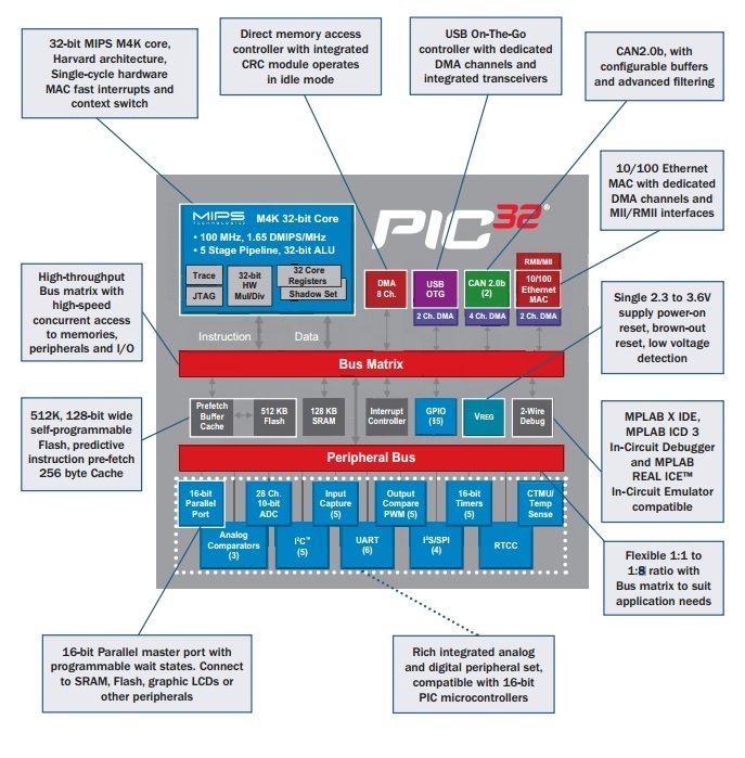
The PIC32 is from 32-bit family of wide purpose microcontrollers from Microchip. Technology. It offers 80+ DMIPS performance with a large variety of on-chip peripherals. It occupies industry leading M4K MIPS32 core from MIPS Technologies, Inc. PIC32 microcontrollers are pin-to-pin compatible with PIC24FJ128GA family of 16-bit microcontrollers. In the PIC32 family, all members use programming interface like otherMicro-chip PIC microcontrollers.
Recommended Components
The following components are used in this project or are helpful for building it with a PIC microcontroller.
| Component | How it’s used in this project | Buy on Amazon |
|---|---|---|
| PIC32 microcontroller (PIC32MX250F128B) | Main 32-bit MCU covered in this tutorial; runs the example code and peripherals. | Check Price |
| PICkit 5 programmer/debugger | Programs and debugs the PIC32 over the ICSP interface. | Check Price |
| Breadboard | Solderless base for wiring the PIC32 and support circuitry. | Check Price |
| Jumper Wires | Connect the MCU pins, power rails and peripherals on the breadboard. | Check Price |
As an Amazon Associate we earn from qualifying purchases. Prices and availability are accurate as of the date/time indicated and are subject to change.
PIC32 microcontroller series
PIC32 microcontroller has two main series.- PIC32MX devices
- PIC32MZ devices
PIC32 microcontrollers features
The PIC32 family offers a number of quality ingredients to enable a large variety of applications.The following section list grouped all the key features in major categories.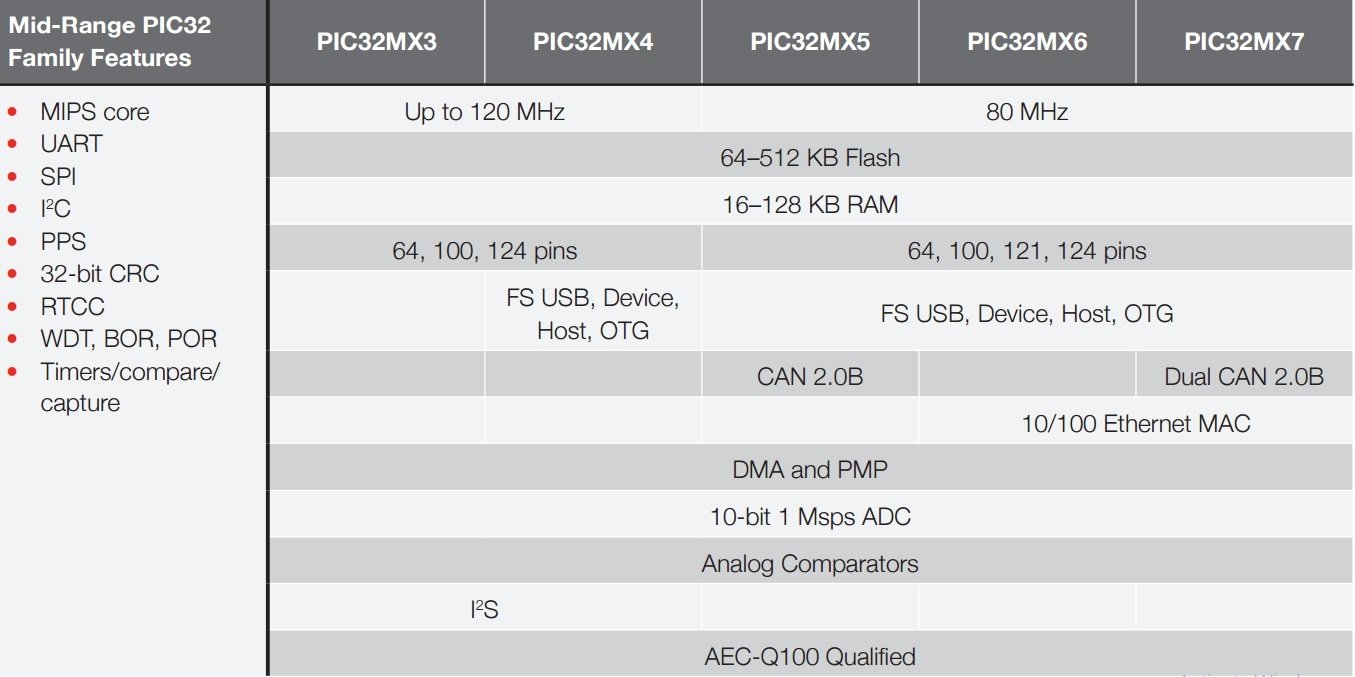
Scalability:
- Industry known MIPS32 compatible M4K CPU core with 5(v) stage pipeline
- It’s pin compatible with 64/100 pin PIC24FJXXXGA family of 16-bit microcontrollers
- It has large family of devices with Flash memory options from 32 KB to 512 KB
Power Management:
- It works from 2.3 to 3.6V
- There are numerous clock sources
- There are various low-power modes including RUN, IDLE and SLEEP
- In it, I/O transfer occurs via DMA in IDLE mode
- In it, programmable peripheral clock is also work
- There is operation during IDLE mode and Individual peripheral do control ON/OFF
- It has full-speed operation over entire voltage range
Performance:
- Up to 80 MHz, MIPS M4K 32-bit core with 5 (v) stage pipeline
- We can calculate it; high-performance hardware multiply/divide unit 1 multiply/clock
- Multiple register sets for reduced disrupt latency
- Programmable user and kernel memory divide for enhanced application stability
- Hardware assist single cycle register bits manipulations
- To shorten individual instruction fetches time, 128-bit wide Flash memory used
- 256 bytes of high-speed cache memory with useful instructions and ROM data prefetch buffer
- Available DMA controller with pattern based transfer termination and integrated CRC calculation
- Includes USB On-The -Go controller for USB device dual-role, or host applications
- USB controller has its own dedicated DMA interface
PIC32 ARCHITECTURE
The PIC32 family joins the MIPS M4K core with embedded Flash, powerful peripherals and RAM memory to address a wide range of applications.
Processor core:
- For interrupt handlers, GPR shadow registers to minimize latency
- Bit field manipulation instruction
- High performance Multiply by Divide Unit-The maximum issue rate of one 32×16 multiply /clock
- The maximum issue rate of one 32×32 multiply every other clock
- Its static implementation is minimum operating frequency 0 MHz
- Low power modes including IDLE, RUN and SLEEP
- MIPS M4K with 5 (v) stage pipeline
- MIPS32-compatible Release 2 (II) Instruction Sets
- MIPS16e™ Code Compression to improve its code density up to 40%
- 2.3 to 3.6V operation with full speed over entire set or rang
DMA Controller:
- It has up to 4 independent channels
- Memory-to-Peripheral, Memory-to-Memory, and Peripheral-to-Memory transfers
- Integrated programmable CRC engine: calculates on the fly at the time when the data is transferred.
- Programmable activation from any IRQ
- Chainable channels, Auto-Enable mode, stop on match detection
- Data transfers while the core is in IDLE mode
Memory:
- It has 4GB virtual memory space
- Fixed Memory Mapping Translation mechanism
- User accessible memory segments for increased application stability Flexible partitioning into kernel
Core Timer:
- It has 32-bit timer in CPU for applying a timer interrupt function.
Debug and Programming:
- Read or write access to SFRs and all data RAM without stopping CPU
- Instruction Trace Port:
- 5 Wire which is non intrusive trace port
- activated by complex breakpoints logic block
- 2 data breakpoints and 6 instructions
- 2 complex breakpoint logic blocks with primed breakpoint triggers, stopwatch timers, Pass counters.
- 2 wire Microchip interface and 4 wire EJTAG
- 2 wire Microchip Interface:
- 6 real-time read or write capture logic blocks
RTCC (Real-Time Clock and Calendar):
- In it time is with hours, minutes and seconds
- And calendar with weekdays, dates, months and years
- And leap year detection as well
- It has highly configurable alarm
- Calibration is up to 260 pm of crystal error
Pre Fetch Cache:
- In it 16 lines, each 128-bit wide, and instruction Prefetch buffer
- And it has ability to lock and load lines which is useful to create SW breakpoints in Flash and have ability to minimize interrupt latency
Interrupt Controller:
- Highest priority interrupt has a specific register set to minimize interrupt latency
- Sub priorities and Multiple priorities for each vector
- Fully programmable interrupt controller is there with Single or Multi vector mode, which can support up to 95 IRQs.
Enhanced Parallel Master Port:
- 8-bit and 16-bit data interface
- It has expandable using GPIO lines and up to 16-bit address lines
- 2 (II) Chip Select lines
Communication channels:
- USB 2.0 compliant (FS 12 Mbps), Host and Device only capable
- 2 Master/Slave/Frame approach SPI channels
- 2 UART channels with hardware IrDA
- 10/7 bits mode addressing, 2 Master/Slave I2C channels, broadcast capable
Analog-to-Digital Converters:
- 8 result alignment options
- Operation would be in running during CPU Sleep mode
- Software selectable External and Internal voltage reference
- It has automatic Channel Scan mode
- Up to 16 Channels, each 10-bit resolution ADCs
- The conversion speed is up to 500+ k samples / second (ksps)
- It has choose able conversion trigger source
- And it has16 words conversion result buffer
- Choose able Buffer Fill modes
Timers:
- 5 16-bit timer/counter ability to form up to 2, 32-bit timer/counters
- It has software choose able internal or external clock source
- It has external pulse counter
- Software chooses able prescalers.
- It is operational in CPU Sleep mode
- Asynchronous timer/counter with a built-in oscillator
- Programmable interrupt priority and generation