Learn to interface 74HC595 with a 7-segment display and Pic microcontroller. By using a 74HC595 shift register to drive 7-segment displays with PIC16F877A microcontroller, we can save GPIO pins of PIC microcontroller. In this tutorial, we learn to interface single-digit and 4-digit 7-segment with PIC16F877A microcontroller using a serial-in and parallel-out shift register IC.
Why do We need to Use 74HC595?
In the last tutorial on 7-segment display interfacing with PIC16F87A, we have seen that if we interface one 7-segment device directly with Pic microcontroller, we will need 8 GPIO pins of MCU. Similarly, if we use two-digital, three-digit, four-digit seven-segment displays, we will need more GPIO pins, even if we use the multiplexing techniques to save microcontroller pins.
Therefore, by using a 74HC595 serial shift register, we can save MCU GPIO pins and can use them for other purposes. For instance, if we use this serial shift register IC, we can interface 7-segment with PIC16F877A by using three pins only, instead of using 8 GPIO pins.
Prerequisites
In order to fully understand this tutorial, you should know about these concepts:
First, you should know how to use digital output pins of PIC16F877A
Secondly, you should understand working and pinout of this IC:
74HC595 Pinout Working and Applications
In the last tutorial, we have seen how to interface 74HC595 with a pic microcontroller. In that post, we controlled 8 LEDs with this shift register IC and by using only three digital output pins of PIC16F877A microcontroller.
74HC595 Interfacing with PIC16F877A microcontroller
74HC595 Interfacing with 7-segments
For demonstration, we will take two example. Firstly, we will interface a single-digit device. Secondly, we will learn to interface 4-digit seven-segment display using 74HC595.
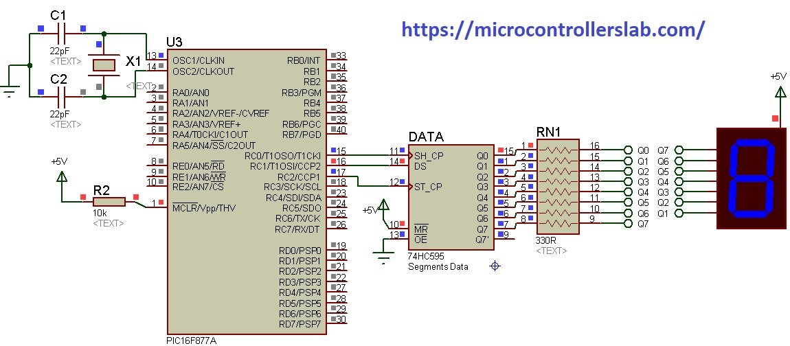
Single-digit 7-Segment Interfacing Schematic Diagram
This schmatic diagram shows the connection between shift regiser IC, PIC16F877A and common anode type single-digit seven-segment.
If you have already above mentioned posts and especially shift register interfacing with PIC16F877A, you should understand this schematic diagram easily except for 7-segment connections.
As you can see from the schematic diagram, we connect 74HC595 with the display unit in reverse order of (Q0-Q7) output pins according to this table.
| 74HC595 | 7-Segment pins |
|---|---|
| Q7 | A |
| Q6 | B |
| Q5 | C |
| Q4 | D |
| Q3 | E |
| Q2 | F |
| Q1 | G |
| Q0 | DP |
This is because shift register first outputs MSB bit and LSB at the end. Therefore, we connect Q7 to a, Q6 to b and so on. Q0 output is not used because it will be used to drive dp pin of the 7-segment device. If your device has dp pin also, connect Q0 pin with dp pin.
Mikroc Code single-digit display
This code is written using MikroC for Pic compiler. Create a new project with MikroC compiler by selecting PIC16F877A microcontroller and set frequency to 8MHz. If you don’t know how create new project in mikroC, we suggest you read this post:
sbit DATA_pin at  PORTC.B1;
sbit LATCH_pin at PORTC.B2;
sbit CLCOK_pin at PORTC.B0;
unsigned char binary_pattern[]={0xC0,0xF9,0xA4,0xB0,0x99,0x92,0x82,0xF8,0x80,0x90};
unsigned int counter=0;
void clock_signal(void){
   CLCOK_pin = 1;
    delay_us(500);
   CLCOK_pin = 0;
    delay_us(500);
}
void latch_enable(void)
   {
    LATCH_pin = 1;
    delay_us(500);
    LATCH_pin = 0;
    }
void send_data(unsigned int data_out)
{
    int i;
    unsigned hold;
    for (i=0 ; i<8 ; i++)
    {
        DATA_pin = (data_out >> i) & (0x01);
        clock_signal();
    }
    latch_enable(); // Data finally submitted
}
void main()
{
  TRISC.B0 = 0; // Set  DATA_pin as output pin
  TRISC.B1 = 0; // Set  CLCOK_pin as output pin
  TRISC.B2 = 0; // Set LATCH_pin as output pin
  while(1)
      {
         send_data(binary_pattern[counter]);
         counter++;
         if(counter>9)
         counter =0;
         delay_ms(1000);
      }
}
How Code works?
This code works similarly to the code of 74HC595 interfacing with PIC16F877A microcontroller except for the “while” loop part. First, we initialize the display codes for common anode type seven-segment display using an array.
unsigned char binary_pattern[]={0xC0,0xF9,0xA4,0xB0,0x99,0x92,0x82,0xF8,0x80,0x90};Inside the while loop, we pass display codes values to send_data() function with the help of a counter variable. Counter variable increments after every one second and used to display updated value. When counter value becomes equal to 9, we reset the counter value to zero.
 send_data(binary_pattern[counter]);
         counter++;
         if(counter>9)
         counter =0;
         delay_ms(1000);
MPLAB XC8 Code Single-Digit Display
This code is for MPLAB XC8 Compiler. If you don’t know how to use MPLAB and XC8 compiler, you can read this complete in-depth guide:
// CONFIG
#pragma config FOSC = HS        // Oscillator Selection bits (HS oscillator)
#pragma config WDTE = OFF        // Watchdog Timer Enable bit (WDT enabled)
#pragma config PWRTE = OFF      // Power-up Timer Enable bit (PWRT disabled)
#pragma config BOREN = OFF       // Brown-out Reset Enable bit (BOR enabled)
#pragma config LVP = ON         // Low-Voltage (Single-Supply) In-Circuit Serial Programming Enable bit (RB3/PGM pin has PGM function; low-voltage programming enabled)
#pragma config CPD = OFF        // Data EEPROM Memory Code Protection bit (Data EEPROM code protection off)
#pragma config WRT = OFF        // Flash Program Memory Write Enable bits (Write protection off; all program memory may be written to by EECON control)
#pragma config CP = OFF         // Flash Program Memory Code Protection bit (Code protection off)
#include <xc.h>
#define DATA_pin PORTCbits.RC1
#define LATCH_pin  PORTCbits.RC2
#define CLCOK_pin  PORTCbits.RC0
#define _XTAL_FREQ 8000000 //Crystal Frequency, used in delay
unsigned char binary_pattern[]={0xC0,0xF9,0xA4,0xB0,0x99,0x92,0x82,0xF8,0x80,0x90};
unsigned int counter=0;
void clock_signal(void){
   CLCOK_pin = 1;
    __delay_us(500);
   CLCOK_pin = 0;
    __delay_us(500);
}
void latch_enable(void)
   {
    LATCH_pin = 1;
    __delay_us(500);
    LATCH_pin = 0;
    }
void send_data(unsigned int data_out)
{
    int i;
    for (i=0 ; i<8 ; i++)
    {
        DATA_pin = (data_out >> i) & (0x01);
        clock_signal();
    }
    latch_enable(); // Data finally submitted
}


void main(void)
{
  TRISC0 = 0; // Set  DATA_pin as output pin
  TRISC1 = 0; // Set  CLCOK_pin as output pin
  TRISC2 = 0; // Set LATCH_pin as output pin
    while(1)
      {
       send_data(binary_pattern[counter]);
         counter++;
         if(counter>9)
         counter =0;
         __delay_ms(1000);

      }
  return;
}
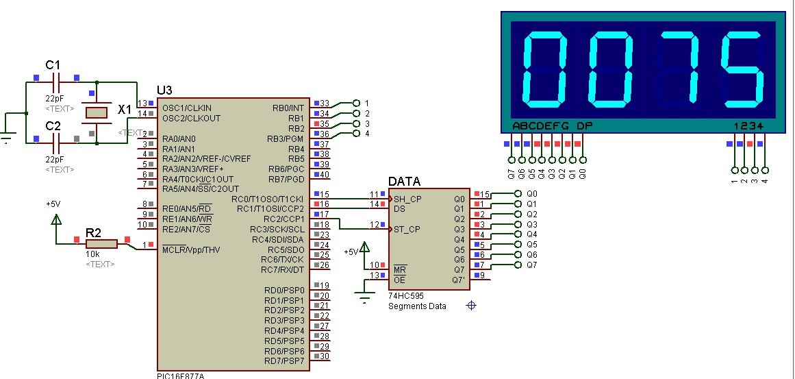
4-Digit 7-segment Display Interfacing Schematic
This schematic shows the interfacing of a 4-digit 7-segment display with a 74HC595 shift register and PIC16F877A microcontroller. As you can see from this schematic diagram, by using 74HC595, we saved 5 GPIO pins of PIC16F877A microcontroller that is used to drive 4-digit seven-segment display. Shift register IC used to send digit display code to the 7-segment device and 4 GPIO pins (RB0-RB3) controls each digit display.
MikroC Code
sbit digit1 at PORTB.B0;
sbit digit2 at PORTB.B1;
sbit digit3 at PORTB.B2;
sbit digit4 at PORTB.B3;
sbit DATA_pin at  PORTC.B1;
sbit LATCH_pin at PORTC.B2;
sbit CLCOK_pin at PORTC.B0;
unsigned char binary_pattern[]={0xC0,0xF9,0xA4,0xB0,0x99,0x92,0x82,0xF8,0x80,0x90};
unsigned int counter=0;
unsigned int a1,a2,a3,a4; // temporary variables to store data of adc
void clock_signal(void){
   CLCOK_pin = 1;
    delay_us(500);
   CLCOK_pin = 0;
    delay_us(500);
}
void latch_enable(void)
   {
    LATCH_pin = 1;
    delay_us(500);
    LATCH_pin = 0;
    }
void send_data(unsigned int data_out)
{
    int i;
    unsigned hold;
    for (i=0 ; i<8 ; i++)
    {
        DATA_pin = (data_out >> i) & (0x01);
        clock_signal();
    }
    latch_enable(); // Data finally submitted
}
void main()
{
  TRISC.B0 = 0; // Set  DATA_pin as output pin
  TRISC.B1 = 0; // Set  CLCOK_pin as output pin
  TRISC.B2 = 0; // Set LATCH_pin as output pin
  TRISB=0x00;
  PORTB = 0X00;
  digit1 = 0;
  digit2 = 0;
  digit3 = 0;
  digit4 = 0;
  while(1)
      {
         a1 = counter / 1000;   // holds 1000's digit
         a2 = ((counter/100)%10); // holds 100's digit
         a3 = ((counter/10)%10);  // holds 10th digit
         a4 = (counter%10);  // holds unit digit value
         send_data(binary_pattern[a1]); // send 1000's place data to fourth digit
        digit1=1;   //  turn on forth display unit
        delay_ms(3);
        digit1=0;   //  turn off forth display unit
        send_data(binary_pattern[a2]);  // send 100's place data to 3rd digit
        digit2=1;    //  turn on 3rd display unit
        delay_ms(3);
        digit2=0;  //  turn off 3rd display unit
        send_data(binary_pattern[a3]);  // send 10th place data to 2nd digit
        digit3 = 1;  //  turn on 2nd display unit
        delay_ms(3);
       digit3 = 0;   //  turn off 2nd display unit
       send_data(binary_pattern[a4]);  // send unit place data to 1st digit
       digit4 = 1;  //  turn on 1st display unit
       delay_ms(3);
       digit4 = 0;  //  turn off 1st display unit
         counter++;
         if(counter>9999)
         counter =0;
         //delay_ms(1000);
      }
}
MPLAB XC8 Code
// CONFIG
#pragma config FOSC = HS        // Oscillator Selection bits (HS oscillator)
#pragma config WDTE = OFF        // Watchdog Timer Enable bit (WDT enabled)
#pragma config PWRTE = OFF      // Power-up Timer Enable bit (PWRT disabled)
#pragma config BOREN = OFF       // Brown-out Reset Enable bit (BOR enabled)
#pragma config LVP = ON        // Low-Voltage (Single-Supply) In-Circuit Serial Programming Enable bit (RB3/PGM pin has PGM function; low-voltage programming enabled)
#pragma config CPD = OFF        // Data EEPROM Memory Code Protection bit (Data EEPROM code protection off)
#pragma config WRT = OFF        // Flash Program Memory Write Enable bits (Write protection off; all program memory may be written to by EECON control)
#pragma config CP = OFF         // Flash Program Memory Code Protection bit (Code protection off)
#include <xc.h>
#define DATA_pin PORTCbits.RC1
#define LATCH_pin  PORTCbits.RC2
#define CLCOK_pin  PORTCbits.RC0
#define digit1 PORTBbits.RB0
#define digit2 PORTBbits.RB1
#define digit3 PORTBbits.RB2
#define digit4 PORTBbits.RB3
#define _XTAL_FREQ 2000000 //Crystal Frequency, used in delay
unsigned char binary_pattern[]={0xC0,0xF9,0xA4,0xB0,0x99,0x92,0x82,0xF8,0x80,0x90};
unsigned int counter=0;
unsigned int a,b,c,d;
void clock_signal(void){
   CLCOK_pin = 1;
    __delay_us(500);
   CLCOK_pin = 0;
    __delay_us(500);
}
void latch_enable(void)
   {
    LATCH_pin = 1;
    __delay_us(500);
    LATCH_pin = 0;
    }
void send_data(unsigned int data_out)
{
    int i;
    for (i=0 ; i<8 ; i++)
    {
        DATA_pin = (data_out >> i) & (0x01);
        clock_signal();
    }
    latch_enable(); // Data finally submitted
}


void main(void)
{
  TRISC0 = 0; // Set  DATA_pin as output pin
  TRISC1 = 0; // Set  CLCOK_pin as output pin
  TRISC2 = 0; // Set LATCH_pin as output pin
  TRISB=0X00;
  digit1 = 0;
  digit2 = 0;
  digit3 = 0;
  digit4 = 0;
    while(1)
      {

         a = counter / 1000;   // holds 1000's digit
         b = ((counter/100)%10); // holds 100's digit
         c = ((counter/10)%10);  // holds 10th digit
         d = (counter%10);  // holds unit digit value
         send_data(binary_pattern[a]); // send 1000's place data to fourth digit
        digit1=1;   //  turn on forth display unit
        __delay_ms(10);
        digit1=0;   //  turn off forth display unit
        send_data(binary_pattern[b]);  // send 100's place data to 3rd digit
        digit2=1;    //  turn on 3rd display unit
        __delay_ms(10);
        digit2=0;  //  turn off 3rd display unit
         send_data(binary_pattern[c]);  // send 10th place data to 2nd digit
         digit3 = 1;  //  turn on 2nd display unit
         __delay_ms(10);
        digit3 = 0;   //  turn off 2nd display unit
       send_data(binary_pattern[d]);  // send unit place data to 1st digit
       digit4 = 1;  //  turn on 1st display unit
       __delay_ms(10);
       digit4 = 0;  //  turn off 1st display unit

     if(counter>=9999) //wait till flag reaches 100
         {
         counter=0; //only if flag is hundred "i" will be incremented
         }
         counter++; //increment flag for each flag
     }

  return;
}
Simulation Result
Related content:
- 7 Segment Display Interfacing with Pic Microcontroller
- MAX7219 Interfacing with 8-digit 7 Segment Display and PIC16F877A
- LM35 Temperature Sensor with 7-Segment Display using Pic Microcontroller
- Digital DC Voltmeter using 7-Segment Display and Pic Microcontroller
- Display ADC value on 4-digit 7-Segment Display using Pic Microcontroller