In this tutorial, we will go through an analog to digital converter or ADC module of pic microcontrollers. Almost all pic microcontroller series such as PIC10F, PIC12F, PIC16F, PIC18F, and PIC32 controllers have built ADC Modules. But its size depends on the device from which category/ series, you are using. In this tutorial, we will see the ADC module of the PIC18F series. But the concepts are almost the same for every device except some changes to the names of internal ADC registers. Most importantly, we can easily check registers names from the microcontroller datasheet.
PIC18F ADC Module
Firstly, all PIC18F series has a built-in 10-bit ADC module. Each microcontroller can accept up to 16 analog inputs. In other words, it can have up to sixteen ADC channels. But the actual number of channels depends on the microcontroller, you are using. However, control and configurations registers are the same for every PIC18F series microcontrollers.
How PIC18F ADC Works?
ADC mainly consists of charge/hold capacitor and successive approximation converter. Firstly, each channel accepts analog inputs which charges charge and hold capacitor. The output of charge/hold capacitor feds to an input of the digital converter. After that, a digital converter changes analog value into a 10-bit digital value. This digital value is equivalent to its analog input signal. The A/D conversion technique uses a successive approximation (SAR) technique.

Please refer to this Analog to Digital Converter Article, to understand its working.
PIC18F ADC Block Diagram

PIC18F ADC Registers
Pic microcontroller analog to digital converter module has five registers. We use these registers to configure features such as sampling rate, A/D clock, channel selection, voltage reference for ADC and format of result that how the result will be stored. We will see details of all these features later on.
- ADRESH Register: This register stores higher or lower bits of digital conversion result after the A/D converter produces a 10-bit digital number. Therefore, it stores 2 higher/lower bits of 10-bit digital number depending on how we justified the result storage rule.
- ADRESL Register: Similarly, ASREDL holds 8 least significant bits or most significant bits of 10-bit digital number that is an output of A/D converter or SAR.
Note: ADFM bit of ADCON2 Register determines either the result will be left-justified or right-justified. For further information refer to the ADCON2 register section.
ADCON0 – ADC Control Register 0
The ADCON0 register stands for Analog to digital converter control register zero. ADCON0 has 8 bits and 2 bits (bit 6-7) have no connection or unused.

- Firstly, it selects the analog input channel from CH0-CH15 with the help of CHS3: CHS0 bits. We configure these four bits ( from bit 2-5) to select a specific channel. For example, if we set these four bits to zero:
 CHS3=0;
 CHS2=0;
 CHS1=0;
 CHS0=0;
This configuration will select analog channel zero or AN0 to get an analog signal from.
- Bit zero ADON starts of stops the ADC. Therefore, before using this module, we should turn on this bit by setting ADON=1. It is recommended to turn off ADC by setting this bit to zero if you are not using ADC. Because it will save power.
- Bit one GO/~DONE shows the status of A/D conversion. Hence, we can use this bit as a flag bit to find either A/D conversion is in progress or completed.
ADCON1 – ADC Control Register 1
ADCON1 register has two functions. First, all GPIO ports of pic microcontroller have multiple functions. For example, we can use the same port either as a digital pin or analog pin. But we can use only one function at a time. Therefore, we can select pins functionality either as a digital or ADC pin with this register. Additionally, this register also used to select reference voltage for A/D converter.

- Bit number 6-7 are unused. Even if a programmer tries to read them, they will be read as a zero.
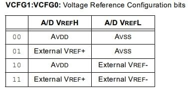
- From Bit 0-3 PCFG3: PCFG0 are port pins configuration control bits. These least significant bits of ADCON1 configure which pin will work as a digital or which pin will work as an analog input pin. For instance, setting these bits to zero will configure all pins as analog pins. For further setting check this table:

- Bit 4 and 5 of ADCON1 register namely, VCFG1: VCFG0 are reference voltage configuration bits for the ADC module. Reference voltage defines the range of voltage that we can measure with this A/D module. But the maximum value of the range depends on the operating voltage or VDD of the pic microcontroller. Therefore, with these bits, we can select either internal or external reference voltage. For more information on the Reference voltage, see the ADC resolution section.
ADCON2 – ADC Control Register 2
ADCON2 is last a register used to configure ADC of pic microcontroller. This register selects A/D module conversion clock input. In other words, it selects conversion frequency. Furthermore, this register defines the format of 10-bit digital value either as a left-justified or right-justified.

- ADCON2 register bit 2-0 used to select clock frequency. The name of these bits is ADCS2: ADCS0.
- ADFM Bit defines the format of the ADC result. This result stores in ADRESL and ADRESH registers according to the defined format.
- ACQT2: ACQT0: These bits set the time of ADC acquisition which is a time required to charge and discharge charge holding capacitor.
PIC Microcontroller ADC Resolution
Usually, we define its performance with two important factors. One is resolution and the second one is speed. In this section, we will talk about resolution. Next, we go through the speed of A/D conversion.

What is Resolution?
The resolution of an ADC is the most important concept that defines the minimum level of voltage we can measure with it. In other words, what is the minimum value of the voltage that increments the digital value by one? For example, the pic microcontroller has a 10-bit ADC. It means, the digital value can go up to 0-1023. Resolution defines minimum required voltage that will increment digital value from 0 to 1 and so on.
We can use this formula to define this number:
Resolution = (Vref+ – Vref-)/(2n – 1)
As we have seen in the ADCON1 register section that VCFG1: VCFG0 bits are used to select reference voltage. For instance, we want to use VDD and VSS of the pic microcontroller as a Vref+ and Vref-. We can set these bits as:
ADCON1. VCFG1= 0;
ADCON1. VCFG0 =0 ;
This configuration selects Vref+ = 5 volts and Vref- =0. ADC of Pic microcontroller is 10-bit wide. Therefore n=10. By putting these values into the above formula:
Resolution= (5-0)/(210 - 1 ) = 5/1023= 0.004887V
Therefore, the resolution of the 10-bit A/D converter is 4.88mV. In short, a 10-bit ADC of pic microcontroller will detect 4.88mV as a digital one and 4.88×2 = 9.66mV as a digital two and so on.
Note: It has a minimum resolution of 4.88mV that means this A/D module cannot differentiate between 1mV, 2mV, and 3mV. It will detect all these values as a digital zero. That means, the more resolution we have, smaller the voltage, a module can measure.
How to increase Resolution?
According to this formula, there are two ways to increase the resolution of ADC:
Resolution = (Vref+ – Vref-)/(2n – 1)
- By increasing the number of bits
- By Changing reference voltage.
ADC Acquisition Time PIC Microcontroller
ADC acquisition time depends on the charging time of the charge hold capacitor. Before acquiring data from the A/D module, a charge hold capacitor should be fully charged according to the magnitude of an input voltage. A charge acquisition time can vary for different pic microcontrollers. You can refer to the datasheet of a specific microcontroller to know about its minimum time requirement.
Charge holding time depends on the following factors:
- capacitor value
- Input impedance
- Vdd
- Conversion error
- Temperature
But we don’t need to worry about these calculations. Because we can get its value directly from the datasheet.
PIC18F4550 ADC Acquisition Time
For example, we will be using the PIC18F4550 microcontroller in this tutorial. According to its datasheet, the minimum required acquisition time is 2.45µs ( Page 272, Equation 21-3). That means after applying an analog input voltage to the analog channel, we should wait for 2.45µs. After that, we can digital data acquisition.
ADC Conversion Clock
ADCON2 register gives use a feature to set acquisition time and clock frequency of ADC. This time starts counting every time we set GO/DONE bit of ADCON0 register. We can set acquisition time with ACQT2: ACQT0.
Now we will see how to select clock frequency for A/D converter. The conversion clock defines the Analog to digital conversion time per bit. It is also known as TAD. Hence the time required for 10 bits will be 10xTAD.
Time TAD depends on the clock frequency of A/D. As mentioned earlier in ADCON2 register section, ADCS2: ADCS0 bits are used to select clock frequency from these possible options:
- 2TOSC
- 4TOSC
- 8TOSC
- 16TOSC
- 32TOSC
- 64TOSC
- Internal A/D RC oscillator
Note: TAD can not be less than the value specified in the datasheet that is 0.8µs for PIC18F4550 microcontroller. For example, if we select 20MHz frequency crystal for a pic microcontroller:
FOSC = 20MHZ
TOSC = 1 / FOSC = 50ns
If we select 8TOSC by setting ADCS2: ADCS0 bits
8 Tosc = 8 x 50ns = 0.4 us
ADC Conversion Operation
To understand the complete A/D conversion operation, check this diagram.

PIC18F4550 Microcontroller ADC Programming
In this section, we will see how to configure ADCON0, ADCON1 and ADCON2 registers to measure analog voltage.
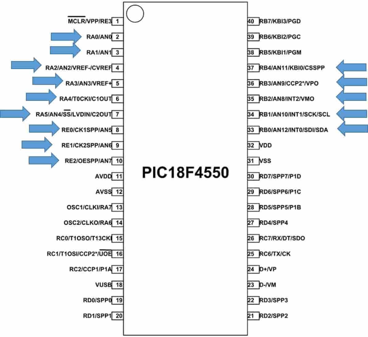
PIC18F4550 ADC Pins
If you see the pinout of PIC18F4550, it has 13 analog input channels AN0-AN12 and each channel is of 10-bit width.
How to Program A/D Module
Now let’s apply all the concepts that we learned in the last section to configure ADC registers of PIC18F4550 microcontroller.
Configure ADCON0
For instance, we want to use channel 0 and enable the ADC module. Now you know that the ADCON0 register sets these features.
ADCON0 = 0b00000001;
This line selects channel AN0. Because we set channel selection bits to zero. Moreover, we enable the ADC module by setting ADON=1. Initially, GO/~DONE bit sets to zero.
We can also write it like this because OR gate operation will make only LSB 1 and other bits to zero.
ADCON0 = ADCON0 | 1 ;
Configure ADCON1
This register sets pins either as a digital or analog pin. We want to use only an AN0 pin as an analog pin. Therefore, we will set ADCON1 register bits 0-3 PCFG3: PCFG0 = 1110. It will set only pin AN0 as an analog pin and the other 12 pins as digital pins.
ADCON1=0b00001110;
Configure ADCON2
For example, we use operating frequency for PIC18F4450 microcontroller. As you know, this register defines ADC clock input, data acquisition time and result format.
ADCON2=0b10011010;
This setting will select the result in a right-justified format ( ADFM=1). Data acquisition time will be 6 TAD. Because of bits 5-3 of ADCON2 ACQT2: ACQT0 = 011. Similarly, ADC clock frequency sets to 32Tosc.
Reading ADC Data
After that, we use GO/~Done bit to check if ADC conversion is completed. If completed we store the result inside any variable.
While(GO_nDone); //wait untill ADC conversion completed
ADC_VALUE=ADRESH<<8)+ADRESL; // store the result inside ADC_VALUE variable
This is a polling-based method to read ADC value. Because we used a loop to wait until A/D conversion finishes. But we can use interrupt also. We see this method later part of this tutorial.
PIC ADC Programming Steps
Following these steps to initialize registers and to read A/D module values:
- First of all, turn on the A/D module by setting ADCON0bits. ADON=1. It will turn on the ADC Module.
- After that, set the pin as an input using the TRISX direction control register. For example, if you are using analog pin AN0, set TRISAbits.B0=1.
- Select the analog channel using the ADCON0 register.
- After that, set the reference voltage and port configuration bits using the ADCON1 register.
- Set the ADC data acquisition time and clock frequency with the ADCON2 register.
- Wait till data acquisition time finishes by checking to GO/Done pin. We can also use the interrupt method instead of waiting.
- After that read, the values of ADRESL and ADRESH registers that will contain digital 10-bit output.
- Repeat these steps again.
Interfacing POT and LCD with PIC Microcontroller
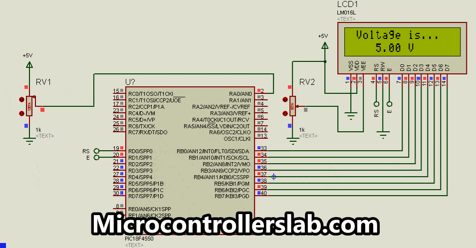
In this section, we will see an example to use the ADC module. For this purpose, we will use a variable resistor to get a variable dc voltage. We will apply this variable dc voltage to AN0 or analog channel zero of PIC18F4550 microcontroller. Moreover, we also use a 16×2 LCD with PORTB and PORTD to display the measured voltage value.

We will not explain the LCD interfacing part of this tutorial. Because we have already posted an article on this:
PIC18F4550 ADC Code in MPLAB XC8
Now let’s see a complete ADC code with an example. For the demonstration purpose, we will use a variable resistor to give a variable input voltage between 0-5 volts to AN0 pin. We will display this voltage on 16×2 LCD.
MPLAB XC8 Compiler Code
We use the MPLAB XC8 compiler to write a pic microcontroller ADC code. If you are a beginner with MPLAB XC8 compiler, you can this getting started guide:
#include <stdio.h>
#include <string.h>
#include <stdlib.h>
#include <P18F4550.h>

// PIC18F4550 Configuration Bit Settings

// 'C' source line config statements

#include <xc.h>

// #pragma config statements should precede project file includes.
// Use project enums instead of #define for ON and OFF.

// CONFIG1L
#pragma config PLLDIV = 1 // PLL Prescaler Selection bits (No prescale (4 MHz oscillator input drives PLL directly))
#pragma config CPUDIV = OSC1_PLL2// System Clock Postscaler Selection bits ([Primary Oscillator Src: /1][96 MHz PLL Src: /2])
#pragma config USBDIV = 1 // USB Clock Selection bit (used in Full-Speed USB mode only; UCFG:FSEN = 1) (USB clock source comes directly from the primary oscillator block with no postscale)

// CONFIG1H
#pragma config FOSC = INTOSC_EC // Oscillator Selection bits (Internal oscillator, CLKO function on RA6, EC used by USB (INTCKO))
#pragma config FCMEN = OFF // Fail-Safe Clock Monitor Enable bit (Fail-Safe Clock Monitor disabled)
#pragma config IESO = OFF // Internal/External Oscillator Switchover bit (Oscillator Switchover mode disabled)

// CONFIG2L
#pragma config PWRT = OFF // Power-up Timer Enable bit (PWRT disabled)
#pragma config BOR = ON // Brown-out Reset Enable bits (Brown-out Reset enabled in hardware only (SBOREN is disabled))
#pragma config BORV = 3 // Brown-out Reset Voltage bits (Minimum setting)
#pragma config VREGEN = OFF // USB Voltage Regulator Enable bit (USB voltage regulator disabled)

// CONFIG2H
#pragma config WDT = OFF // Watchdog Timer Enable bit (WDT disabled (control is placed on the SWDTEN bit))
#pragma config WDTPS = 32768 // Watchdog Timer Postscale Select bits (1:32768)

// CONFIG3H
#pragma config CCP2MX = ON // CCP2 MUX bit (CCP2 input/output is multiplexed with RC1)
#pragma config PBADEN = ON // PORTB A/D Enable bit (PORTB<4:0> pins are configured as analog input channels on Reset)
#pragma config LPT1OSC = OFF // Low-Power Timer 1 Oscillator Enable bit (Timer1 configured for higher power operation)
#pragma config MCLRE = OFF // MCLR Pin Enable bit (RE3 input pin enabled; MCLR pin disabled)

// CONFIG4L
#pragma config STVREN = ON // Stack Full/Underflow Reset Enable bit (Stack full/underflow will cause Reset)
#pragma config LVP = OFF // Single-Supply ICSP Enable bit (Single-Supply ICSP disabled)
#pragma config ICPRT = OFF // Dedicated In-Circuit Debug/Programming Port (ICPORT) Enable bit (ICPORT disabled)
#pragma config XINST = OFF // Extended Instruction Set Enable bit (Instruction set extension and Indexed Addressing mode disabled (Legacy mode))

// CONFIG5L
#pragma config CP0 = OFF // Code Protection bit (Block 0 (000800-001FFFh) is not code-protected)
#pragma config CP1 = OFF // Code Protection bit (Block 1 (002000-003FFFh) is not code-protected)
#pragma config CP2 = OFF // Code Protection bit (Block 2 (004000-005FFFh) is not code-protected)
#pragma config CP3 = OFF // Code Protection bit (Block 3 (006000-007FFFh) is not code-protected)

// CONFIG5H
#pragma config CPB = OFF // Boot Block Code Protection bit (Boot block (000000-0007FFh) is not code-protected)
#pragma config CPD = OFF // Data EEPROM Code Protection bit (Data EEPROM is not code-protected)

// CONFIG6L
#pragma config WRT0 = OFF // Write Protection bit (Block 0 (000800-001FFFh) is not write-protected)
#pragma config WRT1 = OFF // Write Protection bit (Block 1 (002000-003FFFh) is not write-protected)
#pragma config WRT2 = OFF // Write Protection bit (Block 2 (004000-005FFFh) is not write-protected)
#pragma config WRT3 = OFF // Write Protection bit (Block 3 (006000-007FFFh) is not write-protected)

// CONFIG6H
#pragma config WRTC = OFF // Configuration Register Write Protection bit (Configuration registers (300000-3000FFh) are not write-protected)
#pragma config WRTB = OFF // Boot Block Write Protection bit (Boot block (000000-0007FFh) is not write-protected)
#pragma config WRTD = OFF // Data EEPROM Write Protection bit (Data EEPROM is not write-protected)

// CONFIG7L
#pragma config EBTR0 = OFF // Table Read Protection bit (Block 0 (000800-001FFFh) is not protected from table reads executed in other blocks)
#pragma config EBTR1 = OFF // Table Read Protection bit (Block 1 (002000-003FFFh) is not protected from table reads executed in other blocks)
#pragma config EBTR2 = OFF // Table Read Protection bit (Block 2 (004000-005FFFh) is not protected from table reads executed in other blocks)
#pragma config EBTR3 = OFF // Table Read Protection bit (Block 3 (006000-007FFFh) is not protected from table reads executed in other blocks)

// CONFIG7H
#pragma config EBTRB = OFF // Boot Block Table Read Protection bit (Boot block (000000-0007FFh) is not protected from table reads executed in other blocks)

#define RS LATD0 /*PORTD 0 pin is used for Register Select*/
#define EN LATD1 /*PORTD 1 pin is used for Enable*/
#define ldata LATB /*PORTB is used for transmitting data to LCD*/

void LCD_Init();
void LCD_Command(char );
void LCD_Char(char x);
void LCD_String(const char *);
void MSdelay(unsigned int );
void LCD_String_xy(char ,char ,const char*);
void ADC_Init();
int ADC_Read(int);

#define vref 5.00 /*Reference Voltage is 5V*/

void main()
{
char data[10];
int digital;
float voltage;
OSCCON=0x72; /*Set internal Oscillator frequency to 8 MHz*/
LCD_Init(); /*Initialize 16x2 LCD*/
ADC_Init(); /*Initialize 10-bit ADC*/

LCD_String_xy(1,1,"Voltage is...");

while(1)
{
digital = ADC_Read(0);
voltage = digital*((float)vref/(float)1023); /*Convert digital value into analog voltage*/
sprintf(data,"%.2f",voltage); /*It is used to convert integer value to ASCII string*/
strcat(data," V"); /*Concatenate result and unit to print*/
LCD_String_xy(2,4,data); /*send string data for printing*/
MSdelay(500);
}

}

void ADC_Init()
{
TRISA = 0xff; /*set as input port*/
ADCON1 = 0x0e; /*ref vtg is VDD and Configure pin as analog pin*/
ADCON2 = 0x92; /*Right Justified, 4Tad and Fosc/32. */
ADRESH = 0; /*Flush ADC output Register*/
ADRESL = 0;
}

int ADC_Read(int channel)
{
int digital;
ADCON0 =(ADCON0 & 0b11000011)|((channel<<2) & 0b00111100); /*channel 0 is selected i.e (CHS3CHS2CHS1CHS0=0000)
and ADC is disabled i.e ADON=0*/
ADCON0 |= ((1<<ADON)|(1<<GO)); /*Enable ADC and start conversion*/
while(ADCON0bits.GO_nDONE==1); /*wait for End of conversion i.e. Go/done'=0 conversion completed*/
digital = (ADRESH*256) | (ADRESL); /*Combine 8-bit LSB and 2-bit MSB*/
return(digital);
}

void LCD_Init()
{
TRISB = 0;
TRISD=0;
MSdelay(5);
LCD_Command(0x38); /*uses 2 line and initialize 5*7 matrix of LCD*/
LCD_Command(0x01); /*clear display screen*/
LCD_Command(0x06); /*increment cursor (shift cursor to right)*/
LCD_Command(0x0c); /*display on cursor off*/
}

void LCD_Command(char cmd )
{
ldata= cmd; /*Send command to LCD */
RS = 0; /*Command Register is selected*/
EN = 1; /*High-to-Low pulse on Enable pin to latch data*/
MSdelay(1);
EN = 0;
MSdelay(3);
}

void LCD_Char(char dat)
{
ldata= dat; /*Send command to LCD */
RS = 1; /*Data Register is selected*/
EN=1; /*High-to-Low pulse on Enable pin to latch data*/
MSdelay(1);
EN=0;
MSdelay(3);
}

void LCD_String(const char *msg)
{
while((*msg)!=0)
{
LCD_Char(*msg);
msg++;
}

}

void LCD_String_xy(char row,char pos,const char *msg)
{
char location=0;
if(row<=1)
{
location=(0x80) | ((pos) & 0x0f); /*Print message on 1st row and desired location*/
LCD_Command(location);
}
else
{
location=(0xC0) | ((pos) & 0x0f); /*Print message on 2nd row and desired location*/
LCD_Command(location);
}

LCD_String(msg);

}
void MSdelay(unsigned int val)
{
unsigned int i,j;
for(i=0;i<=val;i++)
for(j=0;j<81;j++); /*This count Provide delay of 1 ms for 8MHz Frequency */
}
Simulation Result
As you can see from the simulation, as we change the variable resistor value, the voltage value is also changing on the LCD. The maximum input voltage we provide to POT is 5 volts. Because the pic microcontroller can read a maximum voltage of up to 5 volts. Although, we can use some methods to measure higher voltages also.
PIC18F4550 Microcontroller ADC Value On Interrupt
In the last section, we have seen how to measure A/D values using a polling method. In the polling method, the microcontroller waits until A/D completes its conversion and the microcontroller cannot do any other task at the same time except waiting.
By using an interrupt method, the microcontroller continues to execute the next instructions. But when ADC completes its conversion, interrupt takes place. We can then read the digital value using the interrupt service routine. This is a code using pic microcontroller ADC with interrupt.
#include <xc.h>
#include <stdio.h>
#include <string.h>
#include <stdlib.h>

// CONFIG1L
#pragma config PLLDIV = 1 // PLL Prescaler Selection bits (No prescale (4 MHz oscillator input drives PLL directly))
#pragma config CPUDIV = OSC1_PLL2// System Clock Postscaler Selection bits ([Primary Oscillator Src: /1][96 MHz PLL Src: /2])
#pragma config USBDIV = 1 // USB Clock Selection bit (used in Full-Speed USB mode only; UCFG:FSEN = 1) (USB clock source comes directly from the primary oscillator block with no postscale)

// CONFIG1H
#pragma config FOSC = INTOSC_EC // Oscillator Selection bits (Internal oscillator, CLKO function on RA6, EC used by USB (INTCKO))
#pragma config FCMEN = OFF // Fail-Safe Clock Monitor Enable bit (Fail-Safe Clock Monitor disabled)
#pragma config IESO = OFF // Internal/External Oscillator Switchover bit (Oscillator Switchover mode disabled)

// CONFIG2L
#pragma config PWRT = OFF // Power-up Timer Enable bit (PWRT disabled)
#pragma config BOR = ON // Brown-out Reset Enable bits (Brown-out Reset enabled in hardware only (SBOREN is disabled))
#pragma config BORV = 3 // Brown-out Reset Voltage bits (Minimum setting)
#pragma config VREGEN = OFF // USB Voltage Regulator Enable bit (USB voltage regulator disabled)

// CONFIG2H
#pragma config WDT = OFF // Watchdog Timer Enable bit (WDT disabled (control is placed on the SWDTEN bit))
#pragma config WDTPS = 32768 // Watchdog Timer Postscale Select bits (1:32768)

// CONFIG3H
#pragma config CCP2MX = ON // CCP2 MUX bit (CCP2 input/output is multiplexed with RC1)
#pragma config PBADEN = ON // PORTB A/D Enable bit (PORTB<4:0> pins are configured as analog input channels on Reset)
#pragma config LPT1OSC = OFF // Low-Power Timer 1 Oscillator Enable bit (Timer1 configured for higher power operation)
#pragma config MCLRE = OFF // MCLR Pin Enable bit (RE3 input pin enabled; MCLR pin disabled)

// CONFIG4L
#pragma config STVREN = ON // Stack Full/Underflow Reset Enable bit (Stack full/underflow will cause Reset)
#pragma config LVP = OFF // Single-Supply ICSP Enable bit (Single-Supply ICSP disabled)
#pragma config ICPRT = OFF // Dedicated In-Circuit Debug/Programming Port (ICPORT) Enable bit (ICPORT disabled)
#pragma config XINST = OFF // Extended Instruction Set Enable bit (Instruction set extension and Indexed Addressing mode disabled (Legacy mode))

// CONFIG5L
#pragma config CP0 = OFF // Code Protection bit (Block 0 (000800-001FFFh) is not code-protected)
#pragma config CP1 = OFF // Code Protection bit (Block 1 (002000-003FFFh) is not code-protected)
#pragma config CP2 = OFF // Code Protection bit (Block 2 (004000-005FFFh) is not code-protected)
#pragma config CP3 = OFF // Code Protection bit (Block 3 (006000-007FFFh) is not code-protected)

// CONFIG5H
#pragma config CPB = OFF // Boot Block Code Protection bit (Boot block (000000-0007FFh) is not code-protected)
#pragma config CPD = OFF // Data EEPROM Code Protection bit (Data EEPROM is not code-protected)

// CONFIG6L
#pragma config WRT0 = OFF // Write Protection bit (Block 0 (000800-001FFFh) is not write-protected)
#pragma config WRT1 = OFF // Write Protection bit (Block 1 (002000-003FFFh) is not write-protected)
#pragma config WRT2 = OFF // Write Protection bit (Block 2 (004000-005FFFh) is not write-protected)
#pragma config WRT3 = OFF // Write Protection bit (Block 3 (006000-007FFFh) is not write-protected)

// CONFIG6H
#pragma config WRTC = OFF // Configuration Register Write Protection bit (Configuration registers (300000-3000FFh) are not write-protected)
#pragma config WRTB = OFF // Boot Block Write Protection bit (Boot block (000000-0007FFh) is not write-protected)
#pragma config WRTD = OFF // Data EEPROM Write Protection bit (Data EEPROM is not write-protected)

// CONFIG7L
#pragma config EBTR0 = OFF // Table Read Protection bit (Block 0 (000800-001FFFh) is not protected from table reads executed in other blocks)
#pragma config EBTR1 = OFF // Table Read Protection bit (Block 1 (002000-003FFFh) is not protected from table reads executed in other blocks)
#pragma config EBTR2 = OFF // Table Read Protection bit (Block 2 (004000-005FFFh) is not protected from table reads executed in other blocks)
#pragma config EBTR3 = OFF // Table Read Protection bit (Block 3 (006000-007FFFh) is not protected from table reads executed in other blocks)

// CONFIG7H
#pragma config EBTRB = OFF // Boot Block Table Read Protection bit (Boot block (000000-0007FFh) is not protected from table reads executed in other blocks)

#define RS LATD0 /*PORTD 0 pin is used for Register Select*/
#define EN LATD1 /*PORTD 1 pin is used for Enable*/
#define ldata LATB /*PORTB is used for transmitting data to LCD*/
#define vref 5.00 /*Reference Voltage is 5V*/
char data[10];
long int digital;
float voltage;
void LCD_Init();
void LCD_Command(char );
void LCD_Char(char x);
void LCD_String(const char *);
void MSdelay(unsigned int );
void LCD_String_xy(char ,char ,const char*);
void Delay(unsigned int val)
{
unsigned int i,j;
for(i=0;i<=val;i++)
for(j=0;j<81;j++); /*This count Provide delay of 1 ms for 8MHz Frequency */
}

void __interrupt() myISR()
{

digital = (ADRESH*256) | (ADRESL);
voltage = digital*((float)vref/(float)1023); /*Convert digital value into analog voltage*/
sprintf(data,"%.2f",voltage); /*It is used to convert integer value to ASCII string*/
strcat(data," V"); /*Concatenate result and unit to print*/
LCD_String_xy(2,4,data); /*send string data for printing*/
//Delay(250);
PIR1bits.ADIF==0;
}
void main(void)
{

OSCCON=0x72; /*Set internal Oscillator frequency to 8 MHz*/
TRISC=0;
TRISD=0;
TRISA = 0xff; /*set as input port*/
ADCON0 = ADCON0 | 1;
ADCON1 = 0x0e; /*ref vtg is VDD and Configure pin as analog pin*/
ADCON2 = 0x92; /*Right Justified, 4Tad and Fosc/32. */
ADRESH = 0; /*Flush ADC output Register*/
ADRESL = 0;
PIR1bits.ADIF=0; // A/D Conversion flag bit cleared
PIE1bits.ADIE=1; // Enables A/D interrupt
INTCONbits.PEIE=1; // Enable Peipherals interrupt
INTCONbits.GIE=1; // Enable gloable interrupt
LCD_Init(); /*Initialize 16x2 LCD*/
LCD_String_xy(1,1,"Voltage is...");
ADCON0bits.ADON = 1;
while(1)
{

ADCON0bits.GO = 1;
}
}

void LCD_Init()
{
TRISB = 0;
TRISD=0;
MSdelay(5);
LCD_Command(0x38); /*uses 2 line and initialize 5*7 matrix of LCD*/
LCD_Command(0x01); /*clear display screen*/
LCD_Command(0x06); /*increment cursor (shift cursor to right)*/
LCD_Command(0x0c); /*display on cursor off*/
}

void LCD_Command(char cmd )
{
ldata= cmd; /*Send command to LCD */
RS = 0; /*Command Register is selected*/
EN = 1; /*High-to-Low pulse on Enable pin to latch data*/
MSdelay(1);
EN = 0;
MSdelay(3);
}

void LCD_Char(char dat)
{
ldata= dat; /*Send command to LCD */
RS = 1; /*Data Register is selected*/
EN=1; /*High-to-Low pulse on Enable pin to latch data*/
MSdelay(1);
EN=0;
MSdelay(3);
}

void LCD_String(const char *msg)
{
while((*msg)!=0)
{
LCD_Char(*msg);
msg++;
}

}

void LCD_String_xy(char row,char pos,const char *msg)
{
char location=0;
if(row<=1)
{
location=(0x80) | ((pos) & 0x0f); /*Print message on 1st row and desired location*/
LCD_Command(location);
}
else
{
location=(0xC0) | ((pos) & 0x0f); /*Print message on 2nd row and desired location*/
LCD_Command(location);
}

LCD_String(msg);

}
void MSdelay(unsigned int val)
{
unsigned int i,j;
for(i=0;i<=val;i++)
for(j=0;j<81;j++); /*This count Provide delay of 1 ms for 8MHz Frequency */
}
The above code is similar to the last program except for interrupt service routine and A/D interrupt enable bits.
PIR1bits.ADIF=0; // A/D Conversion flag bit cleared
PIE1bits.ADIE=1; // Enables A/D interrupt
INTCONbits.PEIE=1; // Enable Peipherals interrupt
INTCONbits.GIE=1; // Enable gloable interrupt
When interrupt flag bit of A/D becomes one, it stops the normal execution of PIC18F4550 and jumps to ISR function to read 10-bit digital value.
PIC Microcontroller ADC Based Projects
We can also measure a voltage higher than 5 volts using PIC18F4550 or any pic microcontroller. To measure high voltages either AC or DC, step down converts are used such as voltage dividers, step down transformer. Please check these practical projects that are based Pic microcontroller A/D Converter:
- AC Voltage measurement using Pic microcontroller
- AC Current Measurement using PIC16F877A
- Three-phase Voltage Measurement
- Three-phase AC power measurement
- DC Voltmeter using Pic Microcontroller
- DC Ammeter using Pic microcontroller
Recommended Components
The following components are used in this project or are helpful for building it with a PIC microcontroller.
| Component | How it’s used in this project | Buy on Amazon |
|---|---|---|
| PIC18F4550 microcontroller | Host MCU whose ADC module reads the analog input voltage. | Check Price |
| PICkit 5 programmer/debugger | Flashes the compiled hex file onto the PIC and debugs it. | Check Price |
| 16×2 LCD (parallel) | Displays the digital value converted by the PIC ADC. | Check Price |
| 10kΩ Potentiometer | Sets the LCD contrast (and provides an analog input for testing). | Check Price |
| Breadboard | Solderless base for wiring the PIC and components together. | Check Price |
| Jumper Wires | Connect power, ground and signal lines between the parts. | Check Price |
As an Amazon Associate we earn from qualifying purchases. Prices and availability are accurate as of the date/time indicated and are subject to change.
PIC16F877 ADC Assembly Code

LIST    p=16F877
#include "P16F877.INC"

; Macro to generate a MOVLW instruction that also causes a model break:
break      MACRO arg
           DW    0x3100 | (arg & H'FF')
           ENDM
           cblock 0x20
           count, lc1, lc2;
           endc

           ; Vector for normal start up.
           org     0
           goto    start
           org     4
           goto    inthlr

; Main program starts here:
start      clrw                    ; Clear W.
           movwf   PORTB           ; Ensure PORTB is zero before we enable it.
           movwf   PORTD           ; Ensure PORTD is zero before we enable it.
           movwf   count           ; Reset count value.
           movwf   CCPR1H          ; Clear.
           movwf   CCPR1L          ; Clear.

           ; Set up ports:
           bsf     STATUS,RP0      ; Select Bank 1
           movlw   0xFF		   ; Set W to mask for all inputs.
           movwf   TRISA	   ; set TRISA register as inputs.
           movlw   0x00		   ; Set W to mask for all inputs.
           movwf   TRISA	   ; set TRISA register as inputs.

           bcf     STATUS,RP0      ; Select Bank 1
	   bsf     PORTA,0
	   bcf     PORTA,0
	   bsf     PORTA,0
	   bcf     PORTA,0
           bsf     STATUS,RP0      ; Select Bank 0

           movlw   0xFF		   ; Set W to mask for all inputs.
           movwf   TRISA	   ; set TRISA register as inputs.
           clrf    TRISB           ; Set TRISB register as outputs.
           clrf    TRISD           ; Set TRISD register as outputs.

	   movlw   0x81            ; ADFM=1, all inputs analogue, +VREF enabled.
           movwf   ADCON1          ; Save it.
           bcf     STATUS,RP0      ; Select Bank 0.
           movlw   0xC1		   ; Clock/Channel select and enable.
           movwf   ADCON0          ; Save it.
	   movlw   0x01		   ; Number of loops of 255 clocks.
           call    swait           ; Wait for acquire time.

do_conv    bsf     ADCON0,GO
wait_eoc   btfsc   ADCON0,GO	   ; Is bit still set?
           goto    wait_eoc        ; Yes, so loop and wait for end of conversion.

	   bcf     STATUS,RP0      ; Ensure we have bank 0.
           bsf     PORTD,0         ; Show ISR in progress.
           incf    count,F         ; Increment count.
           call    disp_adc        ; Display captured value.
           bcf     PORTD,0         ; Remove progress bit.

	   movlw   0x40            ; Count
           movwf   count           ; Save it.
loop1      nop                     ; Dilly...
	   nop                     ; Dally...
	   nop                     ; Dilly...
	   decfsz count            ; Decrement loop counter
	   goto loop1              ; Loop if no zero.

	   goto    do_conv	   ; Do another conversion.

disp_adc   bsf     STATUS,RP0      ; Bank 1.
	   movf    ADRESL,W        ; Get ADRESL into W.
           bcf     STATUS,RP0      ; Bank 0.
           movwf   PORTB           ; Write it to port
           bsf     PORTD,6         ; Toggle latch enable
           nop                     ; Wait
           nop                     ; Wait
           bcf     PORTD,6         ; Toggle latch enable
	   movf    ADRESH,W        ; Get ADRESH into W.
	   movwf   PORTB           ; Write it to port
           bsf     PORTD,7         ; Toggle latch enable
           nop                     ; Wait
           nop                     ; Wait
           bcf     PORTD,7         ; Toggle latch enable
           return

inthlr     retfie

; -------------------------------------------------------------------------------
; Wait function
; -------------
swait      movwf   lc2
_sw2       movlw   0xFF
           movwf   lc1
_sw3       nop
           decfsz  lc1,f
           goto    _sw3
           decfsz  lc2,f
           goto    _sw2
           return

           END